

Xem thông số kỹ thuật để biết chi tiết sản phẩm.
S-1009N10I-I4T1U
Basic Information Overview
- Category: Integrated Circuit (IC)
- Use: Power Management
- Characteristics: Low Dropout Voltage Regulator
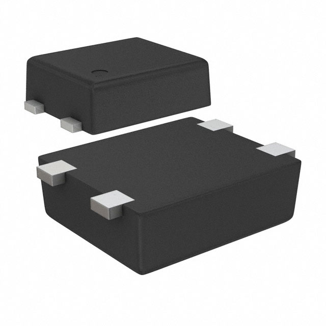
- Package: SOT-23-5
- Essence: Voltage Regulator IC
- Packaging/Quantity: Tape and Reel, 3000 pieces per reel
Specifications
- Input Voltage Range: 2.5V to 6.0V
- Output Voltage Range: 1.0V to 5.5V
- Maximum Output Current: 100mA
- Dropout Voltage: 160mV @ 100mA
- Quiescent Current: 30μA (typical)
- Line Regulation: ±0.05% (typical)
- Load Regulation: ±0.3% (typical)
- Operating Temperature Range: -40°C to +85°C
Detailed Pin Configuration
The S-1009N10I-I4T1U has a total of five pins arranged as follows: 1. VIN: Input voltage pin 2. GND: Ground pin 3. CE: Chip enable pin 4. VOUT: Output voltage pin 5. NC: No connection pin
Functional Features
- Low dropout voltage ensures stable output even with low input voltage.
- Excellent line and load regulation for precise voltage control.
- Low quiescent current minimizes power consumption in standby mode.
- Built-in overcurrent protection safeguards the circuit from excessive current.
Advantages
- Wide input voltage range allows flexibility in various applications.
- Small package size (SOT-23-5) enables space-saving designs.
- Low dropout voltage ensures efficient power conversion.
- Excellent line and load regulation provides accurate voltage output.
Disadvantages
- Limited maximum output current may not be suitable for high-power applications.
- Operating temperature range may restrict usage in extreme environments.
Working Principles
The S-1009N10I-I4T1U is a low dropout voltage regulator that maintains a stable output voltage even when the input voltage drops close to the desired output voltage. It achieves this by utilizing a PNP transistor as a pass element and an error amplifier to compare the output voltage with a reference voltage. The feedback loop adjusts the pass element's resistance to maintain the desired output voltage.
Detailed Application Field Plans
The S-1009N10I-I4T1U is commonly used in various battery-powered devices, such as portable electronics, IoT devices, and wireless communication modules. Its low dropout voltage and low quiescent current make it suitable for applications where power efficiency and extended battery life are crucial.
Detailed and Complete Alternative Models
- S-1009N10I-M5T1U: Similar specifications but in a different package (SOT-23-5).
- S-1009N10I-I3T1U: Lower maximum output current (50mA) but compatible pin configuration.
- S-1009N10I-I5T1U: Higher maximum output current (150mA) with the same pin configuration.
(Note: These alternative models are provided for reference purposes and may have slight variations in specifications.)
This entry provides comprehensive information about the S-1009N10I-I4T1U voltage regulator IC. It covers its basic information, specifications, pin configuration, functional features, advantages, disadvantages, working principles, application field plans, and alternative models.
Liệt kê 10 câu hỏi và câu trả lời thường gặp liên quan đến ứng dụng S-1009N10I-I4T1U trong giải pháp kỹ thuật
Sure! Here are 10 common questions and answers related to the application of S-1009N10I-I4T1U in technical solutions:
Q1: What is S-1009N10I-I4T1U? A1: S-1009N10I-I4T1U is a specific model or type of component used in technical solutions, typically in electronic circuits.
Q2: What is the purpose of S-1009N10I-I4T1U? A2: The purpose of S-1009N10I-I4T1U is to regulate voltage levels within a circuit, ensuring stable and reliable power supply.
Q3: What are the key features of S-1009N10I-I4T1U? A3: Some key features of S-1009N10I-I4T1U include low dropout voltage, high accuracy, low quiescent current, and overcurrent protection.
Q4: What is the input voltage range for S-1009N10I-I4T1U? A4: The input voltage range for S-1009N10I-I4T1U typically varies from 2.5V to 6.0V.
Q5: What is the output voltage range for S-1009N10I-I4T1U? A5: The output voltage range for S-1009N10I-I4T1U can be adjusted between 0.8V and 5.0V.
Q6: Can S-1009N10I-I4T1U handle high currents? A6: Yes, S-1009N10I-I4T1U has a maximum output current capability of 1A, making it suitable for various applications.
Q7: Is S-1009N10I-I4T1U suitable for battery-powered devices? A7: Yes, S-1009N10I-I4T1U is designed to be highly efficient and has a low quiescent current, making it ideal for battery-powered devices.
Q8: Does S-1009N10I-I4T1U have overcurrent protection? A8: Yes, S-1009N10I-I4T1U incorporates overcurrent protection, which helps safeguard the circuit from excessive currents.
Q9: Can S-1009N10I-I4T1U operate in high-temperature environments? A9: Yes, S-1009N10I-I4T1U is designed to operate within a wide temperature range, typically from -40°C to +85°C.
Q10: What are some typical applications of S-1009N10I-I4T1U? A10: S-1009N10I-I4T1U can be used in various technical solutions, including mobile devices, IoT devices, power management circuits, and portable electronics.
Please note that the specific details mentioned above may vary depending on the manufacturer's specifications and datasheet of S-1009N10I-I4T1U.