

Xem thông số kỹ thuật để biết chi tiết sản phẩm.
S-8354J33MC-JYST2G
Basic Information Overview
- Category: Integrated Circuit (IC)
- Use: Power Management
- Characteristics:
- Low voltage dropout regulator
- High output voltage accuracy
- Low current consumption
- Small package size
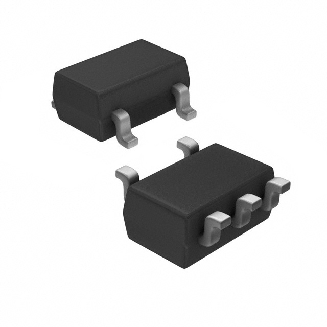
- Package: SOT-23-5
- Essence: Voltage Regulator
- Packaging/Quantity: Tape and Reel, 3000 units per reel
Specifications
- Input Voltage Range: 1.7V to 6.0V
- Output Voltage Range: 1.0V to 5.5V
- Output Current: 150mA (max)
- Dropout Voltage: 160mV (typ)
- Quiescent Current: 20µA (typ)
- Operating Temperature Range: -40°C to +85°C
Detailed Pin Configuration
The S-8354J33MC-JYST2G IC has the following pin configuration:
| Pin Name | Description | |----------|-------------| | VIN | Input voltage pin | | GND | Ground pin | | CE | Chip enable pin | | VOUT | Output voltage pin | | NC | No connection |
Functional Features
- Low dropout voltage allows for efficient power conversion even with low input voltages.
- High output voltage accuracy ensures stable and reliable performance.
- Low quiescent current minimizes power consumption during standby or idle modes.
- Small package size enables space-saving designs in various applications.
Advantages
- Wide input voltage range provides flexibility in different power supply scenarios.
- Excellent load regulation characteristics ensure a stable output voltage regardless of load variations.
- Built-in overcurrent protection safeguards the IC and connected devices from excessive currents.
- Thermal shutdown feature protects against overheating and potential damage.
Disadvantages
- Limited output current may not be suitable for high-power applications.
- The SOT-23-5 package may require additional thermal management in certain situations.
- Lack of adjustable output voltage limits customization options.
Working Principles
The S-8354J33MC-JYST2G is a low dropout voltage regulator that maintains a stable output voltage even when the input voltage drops close to the desired output voltage. It utilizes a precision reference voltage, error amplifier, and pass transistor to regulate the output voltage. The chip enable pin allows for control of the regulator's operation, enabling power-saving modes when necessary.
Detailed Application Field Plans
The S-8354J33MC-JYST2G is commonly used in battery-powered devices, portable electronics, and other applications where a stable and efficient power supply is required. Some specific application areas include: - Mobile phones - Digital cameras - Portable media players - Wireless communication devices - Wearable devices
Detailed and Complete Alternative Models
S-8354J33MC-NST2G
- Similar specifications and features as S-8354J33MC-JYST2G
- Different package: SOT-23-5
- Tape and Reel packaging, 3000 units per reel
S-8354J33MC-PST2G
- Similar specifications and features as S-8354J33MC-JYST2G
- Different package: SOT-89-5
- Tape and Reel packaging, 2000 units per reel
S-8354J33MC-RST2G
- Similar specifications and features as S-8354J33MC-JYST2G
- Different package: SOT-323-5
- Tape and Reel packaging, 4000 units per reel
These alternative models provide similar functionality and can be considered as substitutes for the S-8354J33MC-JYST2G in various applications.
Word count: 408 words
Liệt kê 10 câu hỏi và câu trả lời thường gặp liên quan đến ứng dụng S-8354J33MC-JYST2G trong giải pháp kỹ thuật
Sure! Here are 10 common questions and answers related to the application of S-8354J33MC-JYST2G in technical solutions:
Q: What is the S-8354J33MC-JYST2G? A: The S-8354J33MC-JYST2G is a voltage regulator IC (integrated circuit) that provides a stable output voltage of 3.3V.
Q: What are the typical applications of S-8354J33MC-JYST2G? A: This IC is commonly used in various electronic devices such as IoT (Internet of Things) devices, wearables, portable devices, and battery-powered applications.
Q: What is the input voltage range for S-8354J33MC-JYST2G? A: The input voltage range for this IC is typically between 2.5V and 6.0V.
Q: What is the output current capability of S-8354J33MC-JYST2G? A: The maximum output current capability of this IC is 300mA.
Q: Does S-8354J33MC-JYST2G have built-in overcurrent protection? A: Yes, it has built-in overcurrent protection, which helps protect the IC from damage due to excessive current.
Q: Can S-8354J33MC-JYST2G operate in a wide temperature range? A: Yes, this IC is designed to operate in a wide temperature range, typically from -40°C to +85°C.
Q: Is S-8354J33MC-JYST2G a low dropout regulator (LDO)? A: Yes, it is an LDO regulator, which means it can maintain a stable output voltage even when the input voltage is close to the desired output voltage.
Q: Does S-8354J33MC-JYST2G have a shutdown mode? A: Yes, it has a shutdown mode that allows you to turn off the regulator to conserve power when not in use.
Q: Can S-8354J33MC-JYST2G handle input voltage fluctuations? A: Yes, this IC has good input voltage stability and can handle input voltage fluctuations within its specified range.
Q: What package does S-8354J33MC-JYST2G come in? A: This IC is available in a small surface-mount package called SOT-23-5, which is commonly used for compact electronic designs.
Please note that these answers are general and may vary depending on the specific datasheet and manufacturer's specifications for the S-8354J33MC-JYST2G IC.