

Xem thông số kỹ thuật để biết chi tiết sản phẩm.
AT25DF641A-MH-Y
Product Overview
- Category: Flash Memory
- Use: Data storage and retrieval in electronic devices
- Characteristics: Non-volatile, high-density, low-power consumption
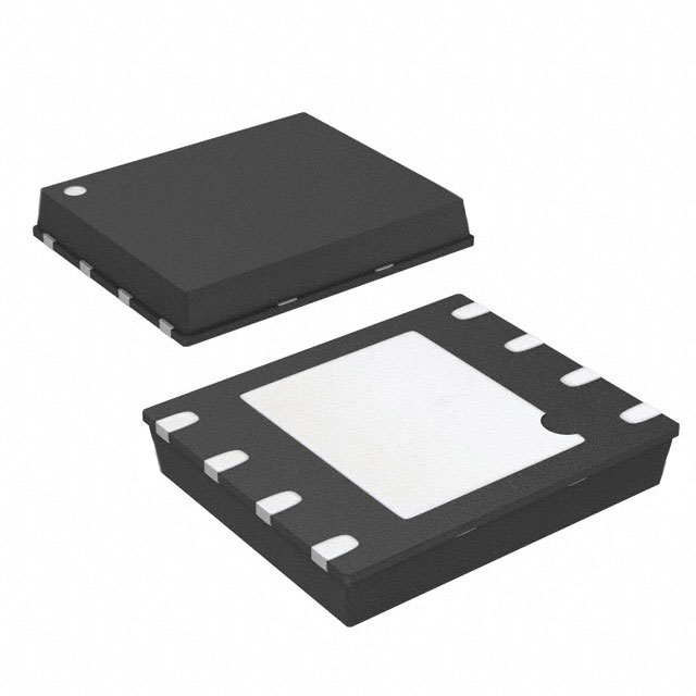
- Package: 8-pin SOIC (Small Outline Integrated Circuit)
- Essence: Serial Peripheral Interface (SPI) Flash memory
- Packaging/Quantity: Tape and reel packaging, 2500 units per reel
Specifications
- Memory Size: 64 Megabits (8 Megabytes)
- Interface: SPI (Serial Peripheral Interface)
- Operating Voltage: 2.7V to 3.6V
- Operating Temperature Range: -40°C to +85°C
- Write Endurance: 100,000 cycles
- Data Retention: 20 years
- Page Size: 256 bytes
- Sector Size: 4 kilobytes
- Block Erase Size: 64 kilobytes
- Read/Program Speed: Up to 85 MHz
Pin Configuration
The AT25DF641A-MH-Y has the following pin configuration:
- Chip Select (/CS)
- Serial Clock (SCK)
- Serial Data Input (SI)
- Serial Data Output (SO)
- Write Protect (/WP)
- Hold (/HOLD)
- VCC (Power Supply)
- Ground (GND)
Functional Features
- High-speed data transfer using SPI interface
- Flexible erase and program operations at page, sector, and block levels
- Low power consumption for extended battery life
- Wide operating temperature range for various environments
- Reliable data retention for long-term storage
- Hardware and software write protection options
- Easy integration into existing systems with standard SPI interface
Advantages
- Compact package size for space-constrained applications
- High-density storage capacity for data-intensive devices
- Fast read/write speeds for efficient data access
- Low power consumption for energy-efficient operation
- Wide operating temperature range for versatile usage scenarios
- Reliable and durable flash memory technology
Disadvantages
- Limited write endurance compared to other non-volatile memory types
- Relatively higher cost per bit compared to traditional hard drives
- Requires additional circuitry for SPI interface implementation
Working Principles
The AT25DF641A-MH-Y operates based on the Serial Peripheral Interface (SPI) protocol. It uses a combination of clock and data signals to communicate with the host device. The flash memory is organized into pages, sectors, and blocks, allowing for flexible erase and program operations. Data is stored in non-volatile memory cells that retain information even when power is removed.
Application Field Plans
The AT25DF641A-MH-Y is widely used in various electronic devices that require non-volatile data storage and retrieval. Some potential application fields include:
- Consumer Electronics: Smartphones, tablets, digital cameras
- Automotive: Infotainment systems, navigation devices
- Industrial: Embedded systems, control units, sensors
- Medical: Patient monitoring devices, diagnostic equipment
- Communication: Routers, modems, network switches
Alternative Models
- AT25DF321A-MH-Y: 32 Megabit (4 Megabyte) version
- AT25DF128A-MH-Y: 128 Megabit (16 Megabyte) version
- AT25DF256A-MH-Y: 256 Megabit (32 Megabyte) version
These alternative models offer different memory sizes to cater to specific application requirements.
Word count: 413 words
Liệt kê 10 câu hỏi và câu trả lời thường gặp liên quan đến ứng dụng AT25DF641A-MH-Y trong giải pháp kỹ thuật
Sure! Here are 10 common questions and answers related to the application of AT25DF641A-MH-Y in technical solutions:
Q: What is the AT25DF641A-MH-Y? A: The AT25DF641A-MH-Y is a serial flash memory chip manufactured by Adesto Technologies.
Q: What is the storage capacity of the AT25DF641A-MH-Y? A: The AT25DF641A-MH-Y has a storage capacity of 64 megabits (8 megabytes).
Q: What is the interface used to communicate with the AT25DF641A-MH-Y? A: The AT25DF641A-MH-Y uses the Serial Peripheral Interface (SPI) for communication.
Q: What voltage levels does the AT25DF641A-MH-Y support? A: The AT25DF641A-MH-Y supports both 3.3V and 2.7V voltage levels.
Q: Can the AT25DF641A-MH-Y be used in industrial applications? A: Yes, the AT25DF641A-MH-Y is designed to operate in industrial temperature ranges (-40°C to +85°C) and is suitable for industrial applications.
Q: Does the AT25DF641A-MH-Y support hardware and software protection features? A: Yes, the AT25DF641A-MH-Y provides hardware and software protection features like write protection, block protection, and security registers.
Q: What is the maximum clock frequency supported by the AT25DF641A-MH-Y? A: The AT25DF641A-MH-Y supports a maximum clock frequency of 104 MHz.
Q: Can the AT25DF641A-MH-Y be used for firmware storage in embedded systems? A: Yes, the AT25DF641A-MH-Y is commonly used for storing firmware, boot code, and other non-volatile data in embedded systems.
Q: Does the AT25DF641A-MH-Y support fast read and dual output read operations? A: Yes, the AT25DF641A-MH-Y supports both fast read and dual output read operations for faster data retrieval.
Q: Is the AT25DF641A-MH-Y compatible with other SPI flash memory chips? A: Yes, the AT25DF641A-MH-Y is compatible with other SPI flash memory chips and can be easily integrated into existing designs.
Please note that these answers are general and may vary depending on specific implementation details and requirements.