

Xem thông số kỹ thuật để biết chi tiết sản phẩm.
AT45DB041E-MHN-Y
Product Overview
Category
AT45DB041E-MHN-Y belongs to the category of flash memory devices.
Use
It is primarily used for data storage and retrieval in various electronic devices.
Characteristics
- Non-volatile memory
- High-speed data transfer
- Low power consumption
- Small form factor
- Reliable and durable
Package
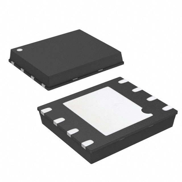
AT45DB041E-MHN-Y is available in a surface-mount 8-pin SOIC package.
Essence
The essence of AT45DB041E-MHN-Y lies in its ability to store and retrieve digital information reliably and efficiently.
Packaging/Quantity
This product is typically packaged in reels, with each reel containing a specific quantity of AT45DB041E-MHN-Y units.
Specifications
- Memory Size: 4 megabits (512 kilobytes)
- Interface: Serial Peripheral Interface (SPI)
- Operating Voltage: 2.7V - 3.6V
- Data Retention: Up to 20 years
- Erase/Write Cycles: 10,000 minimum
Detailed Pin Configuration
- Chip Select (/CS)
- Serial Clock (SCK)
- Serial Data Input (SI)
- Serial Data Output (SO)
- Write Protect (/WP)
- Reset (/RESET)
- VCC (Power Supply)
- Ground (GND)
Functional Features
- Page Program Operation
- Sector Erase Operation
- Block Erase Operation
- Chip Erase Operation
- Continuous Read Mode
- Deep Power-down Mode
- Software Protection
Advantages
- High-speed data transfer allows for efficient read/write operations.
- Low power consumption ensures extended battery life in portable devices.
- Small form factor enables integration into compact electronic devices.
- Reliable and durable, ensuring data integrity over extended periods.
Disadvantages
- Limited memory size may not be sufficient for certain applications.
- Erase/write cycles are limited, which may affect the lifespan of the device.
Working Principles
AT45DB041E-MHN-Y utilizes flash memory technology to store and retrieve digital data. It employs a Serial Peripheral Interface (SPI) for communication with the host device. The memory cells within the device can be programmed, erased, and read using specific commands sent through the SPI interface.
Detailed Application Field Plans
AT45DB041E-MHN-Y finds applications in various electronic devices, including but not limited to: - Smartphones - Tablets - Digital cameras - Portable media players - Automotive systems - Industrial control systems
Detailed and Complete Alternative Models
- AT45DB081E-MHN-Y: 8 megabit flash memory device with similar characteristics and features.
- AT45DB161E-MHN-Y: 16 megabit flash memory device offering increased storage capacity.
- AT45DB321E-MHN-Y: 32 megabit flash memory device suitable for applications requiring larger memory sizes.
(Note: This list is not exhaustive and other alternative models may exist.)
Word count: 410 words
Liệt kê 10 câu hỏi và câu trả lời thường gặp liên quan đến ứng dụng AT45DB041E-MHN-Y trong giải pháp kỹ thuật
Sure! Here are 10 common questions and answers related to the application of AT45DB041E-MHN-Y in technical solutions:
Q: What is the AT45DB041E-MHN-Y? A: The AT45DB041E-MHN-Y is a serial flash memory chip manufactured by Adesto Technologies. It has a capacity of 4 megabits (512 kilobytes) and operates on a serial interface.
Q: What are the typical applications of AT45DB041E-MHN-Y? A: The AT45DB041E-MHN-Y is commonly used in various embedded systems, IoT devices, consumer electronics, and industrial applications that require non-volatile storage for data logging, firmware storage, or code execution.
Q: What is the operating voltage range of AT45DB041E-MHN-Y? A: The AT45DB041E-MHN-Y operates within a voltage range of 2.7V to 3.6V.
Q: What is the maximum data transfer rate supported by AT45DB041E-MHN-Y? A: The AT45DB041E-MHN-Y supports a maximum data transfer rate of up to 85 MHz.
Q: Does AT45DB041E-MHN-Y support hardware or software write protection? A: Yes, the AT45DB041E-MHN-Y supports both hardware and software write protection mechanisms to prevent accidental or unauthorized modification of data.
Q: Can I perform in-system programming (ISP) with AT45DB041E-MHN-Y? A: Yes, the AT45DB041E-MHN-Y supports in-system programming, allowing you to update the contents of the flash memory while it is connected to the target system.
Q: What is the endurance of AT45DB041E-MHN-Y? A: The AT45DB041E-MHN-Y has a typical endurance of 100,000 write cycles per sector.
Q: Does AT45DB041E-MHN-Y have any built-in error correction mechanisms? A: Yes, the AT45DB041E-MHN-Y incorporates hardware-based ECC (Error Correction Code) to ensure data integrity and reliability.
Q: Can I operate multiple AT45DB041E-MHN-Y chips in parallel for increased storage capacity? A: Yes, you can connect multiple AT45DB041E-MHN-Y chips together using the serial interface to achieve higher storage capacities.
Q: Is there any development support available for AT45DB041E-MHN-Y? A: Yes, Adesto Technologies provides documentation, datasheets, application notes, and software libraries to assist developers in integrating and utilizing the AT45DB041E-MHN-Y in their technical solutions.
Please note that these answers are general and may vary depending on specific implementation details or requirements.