

Xem thông số kỹ thuật để biết chi tiết sản phẩm.
AD5362BSTZ
Basic Information Overview
- Category: Integrated Circuit (IC)
- Use: Digital-to-Analog Converter (DAC)
- Characteristics:
- High resolution and accuracy
- Low power consumption
- Small package size
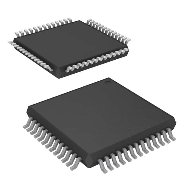
- Package: BSTZ (Thin Shrink Small Outline Package)
- Essence: AD5362BSTZ is a high-performance DAC used for converting digital signals into analog voltages.
- Packaging/Quantity: Available in tape and reel packaging with a quantity of 2500 units per reel.
Specifications
- Resolution: 16-bit
- Number of Channels: 2
- Interface Type: Serial Peripheral Interface (SPI)
- Supply Voltage Range: 2.7V to 5.5V
- Operating Temperature Range: -40°C to +105°C
- Output Voltage Range: 0V to Vref (programmable)
- DNL (Differential Non-Linearity): ±0.5 LSB (max)
- INL (Integral Non-Linearity): ±1 LSB (max)
Detailed Pin Configuration
AD5362BSTZ has a total of 20 pins, which are assigned as follows:
| Pin No. | Pin Name | Description | |---------|----------|-------------| | 1 | VDD | Power supply voltage input | | 2 | VREF | Reference voltage input | | 3 | AGND | Analog ground | | 4 | AOUTA | Analog output channel A | | 5 | AOUTB | Analog output channel B | | 6 | DGND | Digital ground | | 7 | DIN | Serial data input | | 8 | SCLK | Serial clock input | | 9 | SYNC | Chip select input | | 10 | LDAC | Load DAC input | | 11-20 | NC | No connect |
Functional Features
- High-resolution DAC with 16-bit resolution for accurate analog voltage generation.
- Two independent channels (A and B) allow simultaneous conversion of two digital signals.
- Serial Peripheral Interface (SPI) enables easy interfacing with microcontrollers or other digital devices.
- Programmable output voltage range allows flexibility in generating desired analog voltages.
- Low power consumption makes it suitable for battery-powered applications.
- Small package size (BSTZ) saves board space and facilitates compact designs.
Advantages
- High resolution and accuracy ensure precise analog voltage generation.
- Dual-channel capability enables simultaneous conversion of multiple digital signals.
- SPI interface simplifies integration with various digital systems.
- Programmable output voltage range offers versatility in generating different analog voltages.
- Low power consumption prolongs battery life in portable applications.
- Compact package size allows for space-efficient PCB layouts.
Disadvantages
- Limited number of channels may not be sufficient for applications requiring more than two analog outputs.
- The operating temperature range (-40°C to +105°C) may not be suitable for extreme temperature environments.
- Requires external reference voltage (VREF) for proper operation, which adds complexity to the system design.
Working Principles
AD5362BSTZ operates based on the principle of converting digital signals into corresponding analog voltages. It utilizes a 16-bit DAC architecture to achieve high resolution and accuracy. The digital input data is received through the serial interface (DIN, SCLK), and the internal circuitry converts this digital information into analog voltages at the AOUTA and AOUTB pins. The output voltage range can be programmed using the reference voltage (VREF) pin. The LDAC pin allows for simultaneous updating of both DAC outputs.
Detailed Application Field Plans
AD5362BSTZ finds applications in various fields where accurate analog voltage generation is required. Some of the potential application areas include: - Industrial automation and control systems - Test and measurement equipment - Audio processing and synthesis - Programmable power supplies - Motor control systems - Communication devices
Detailed and Complete Alternative Models
- AD5361BSTZ: Similar to AD5362BSTZ but with a single channel instead of dual channels.
- AD5363BSTZ: Higher resolution version with 18-bit DAC architecture.
- AD5364BSTZ: Four-channel version for applications requiring multiple analog outputs.
These alternative models offer different features and specifications, allowing users to choose the most suitable option based on their specific requirements.
In conclusion, AD5362BSTZ is a high-performance DAC that provides accurate analog voltage generation in a compact package. Its high resolution, low power consumption, and dual-channel capability make it suitable for various applications in industrial, audio, and control systems. While it has some limitations, such as limited channels and operating temperature range, there are alternative models available to address different needs.
Liệt kê 10 câu hỏi và câu trả lời thường gặp liên quan đến ứng dụng AD5362BSTZ trong giải pháp kỹ thuật
Sure! Here are 10 common questions and answers related to the application of AD5362BSTZ:
Q: What is the AD5362BSTZ? A: The AD5362BSTZ is a precision, dual-channel, 16-bit digital-to-analog converter (DAC) with integrated voltage reference and output amplifiers.
Q: What is the resolution of the AD5362BSTZ? A: The AD5362BSTZ has a resolution of 16 bits, allowing for high-precision analog output.
Q: What is the voltage reference range of the AD5362BSTZ? A: The AD5362BSTZ has an internal voltage reference range of 2.5V, which can be used as a reference for the DAC outputs.
Q: Can the AD5362BSTZ operate in single-supply mode? A: Yes, the AD5362BSTZ can operate from a single supply voltage ranging from 2.7V to 5.5V.
Q: How many channels does the AD5362BSTZ have? A: The AD5362BSTZ has two independent DAC channels, allowing for simultaneous output of different analog signals.
Q: What is the output voltage range of the AD5362BSTZ? A: The AD5362BSTZ has a programmable output voltage range of 0V to VREF, where VREF is the internal reference voltage.
Q: Can the AD5362BSTZ be controlled using a microcontroller? A: Yes, the AD5362BSTZ has a serial interface (SPI) that allows it to be easily controlled by a microcontroller or other digital devices.
Q: Does the AD5362BSTZ have any built-in diagnostics or fault detection features? A: Yes, the AD5362BSTZ includes a number of diagnostic features such as open-circuit detection and short-circuit protection.
Q: Can the AD5362BSTZ be used in industrial applications? A: Yes, the AD5362BSTZ is suitable for a wide range of industrial applications including process control, instrumentation, and test equipment.
Q: What is the package type of the AD5362BSTZ? A: The AD5362BSTZ is available in a 48-lead LFCSP (lead-frame chip-scale package) which provides compact size and good thermal performance.
Please note that these answers are general and may vary depending on specific application requirements.