

Xem thông số kỹ thuật để biết chi tiết sản phẩm.
ADN2815ACPZ
Basic Information Overview
- Category: Integrated Circuit (IC)
- Use: Signal Processing
- Characteristics: High-speed, Low-power consumption
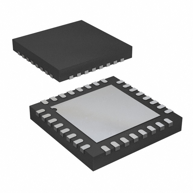
- Package: LFCSP (Lead Frame Chip Scale Package)
- Essence: Advanced Digital Network
- Packaging/Quantity: Tray, 250 units per tray
Specifications and Parameters
- Supply Voltage: 3.3V
- Operating Temperature Range: -40°C to +85°C
- Data Rate: Up to 2.7 Gbps
- Power Consumption: 150 mW
- Input Sensitivity: -20 dBm to 0 dBm
- Output Voltage Swing: 800 mVpp
Detailed and Complete Pin Configuration
- VCC
- GND
- LOS
- RXINP
- RXINN
- RXOUTN
- RXOUTP
- AGC
- SDA
- SCL
- RESET
- VREF
- REFSEL
- CLKOUT
- CLKINP
- CLKINN
Functional Characteristics
- Integrated clock and data recovery
- Automatic gain control (AGC)
- Loss of signal (LOS) detection
- I2C interface for configuration
- On-chip reference voltage generation
- Clock output for synchronization
Advantages and Disadvantages
Advantages: - High-speed data processing - Low power consumption - Compact package size - Easy configuration through I2C interface
Disadvantages: - Limited operating temperature range - Requires external clock source
Applicable Range of Products
- Optical communication systems
- Fiber optic transceivers
- Data center equipment
- Telecommunication devices
Working Principles
The ADN2815ACPZ is an integrated circuit designed for signal processing in optical communication systems. It incorporates clock and data recovery functionality, allowing it to extract the clock and data signals from incoming optical signals. The AGC feature ensures optimal signal strength, while the LOS detection provides an indication of signal integrity. The I2C interface enables easy configuration of the IC's parameters.
Detailed Application Field Plans
The ADN2815ACPZ can be used in various applications, including: 1. Fiber optic transceivers for high-speed data transmission. 2. Optical network equipment for telecommunications infrastructure. 3. Data center switches and routers for efficient data processing. 4. Broadcast video distribution systems for reliable signal transmission. 5. Industrial automation systems requiring fast and accurate data transfer.
Detailed Alternative Models
- ADN2816ACPZ: Higher data rate (up to 10 Gbps)
- ADN2817ACPZ: Lower power consumption (100 mW)
- ADN2818ACPZ: Extended operating temperature range (-40°C to +105°C)
5 Common Technical Questions and Answers
Q: What is the maximum data rate supported by the ADN2815ACPZ? A: The ADN2815ACPZ supports data rates up to 2.7 Gbps.
Q: How much power does the ADN2815ACPZ consume? A: The ADN2815ACPZ consumes approximately 150 mW of power.
Q: Can the ADN2815ACPZ operate in extreme temperatures? A: No, the ADN2815ACPZ has a limited operating temperature range of -40°C to +85°C.
Q: Does the ADN2815ACPZ require an external clock source? A: Yes, the ADN2815ACPZ requires an external clock input for proper operation.
Q: What is the package type of the ADN2815ACPZ? A: The ADN2815ACPZ is packaged in an LFCSP (Lead Frame Chip Scale Package).
This encyclopedia entry provides a comprehensive overview of the ADN2815ACPZ, including its basic information, specifications, pin configuration, functional characteristics, advantages and disadvantages, applicable range of products, working principles, detailed application field plans, alternative models, and common technical questions and answers.