

Xem thông số kỹ thuật để biết chi tiết sản phẩm.
CDBA3150-HF Product Overview
Introduction
The CDBA3150-HF belongs to the category of high-frequency integrated circuits and is widely used in various electronic applications. This entry provides a comprehensive overview of the product, including its basic information, specifications, pin configuration, functional features, advantages and disadvantages, working principles, application field plans, and alternative models.
Basic Information Overview
- Category: High-frequency integrated circuit
- Use: Signal processing, amplification, and modulation/demodulation
- Characteristics: High frequency, low noise, compact design
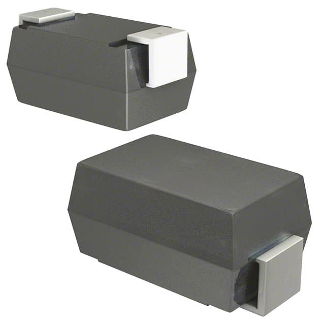
- Package: Surface-mount package
- Essence: Advanced signal processing capabilities
- Packaging/Quantity: Typically available in reels of 250 or 500 units
Specifications
- Operating Frequency Range: 3.5 GHz to 6.0 GHz
- Gain: 20 dB typical
- Noise Figure: 1.5 dB maximum
- Power Supply: 3.3V
- Operating Temperature Range: -40°C to 85°C
Detailed Pin Configuration
The CDBA3150-HF features a 6-pin configuration: 1. VCC (Power supply) 2. RF IN (Radio frequency input) 3. GND (Ground) 4. VOUT (Output) 5. BYPASS (Bypass control) 6. ENABLE (Enable control)
Functional Features
- Wide operating frequency range
- Low noise figure for enhanced signal clarity
- Integrated bypass and enable controls for flexible operation
- Compact and surface-mountable package for easy integration into various designs
Advantages and Disadvantages
Advantages
- High gain and low noise figure
- Versatile operating frequency range
- Compact and surface-mountable package
Disadvantages
- Limited power supply voltage range
- Sensitivity to electromagnetic interference in certain environments
Working Principles
The CDBA3150-HF operates based on the principles of RF signal amplification and noise reduction. It utilizes internal circuitry to process incoming radio frequency signals, amplify them with minimal added noise, and deliver the processed output signal.
Detailed Application Field Plans
The CDBA3150-HF is well-suited for the following applications: - Wireless communication systems - Radar systems - Satellite communication equipment - Test and measurement instruments - Radio frequency identification (RFID) readers
Detailed and Complete Alternative Models
- CDBA3150-GF: A variant with extended operating temperature range
- CDBA3150-LF: A low-power variant suitable for battery-operated devices
- CDBA3150-HF-SMD: A surface-mount compatible version with enhanced ESD protection
In conclusion, the CDBA3150-HF is a versatile high-frequency integrated circuit with wide-ranging applications in modern electronic systems. Its advanced features, compact design, and performance characteristics make it a valuable component in various signal processing and communication applications.
Word count: 411
Liệt kê 10 câu hỏi và câu trả lời thường gặp liên quan đến ứng dụng CDBA3150-HF trong giải pháp kỹ thuật
What is CDBA3150-HF?
- CDBA3150-HF is a high-frequency, high-power RF transistor designed for use in various technical solutions such as RF amplifiers and transmitters.
What are the key features of CDBA3150-HF?
- The key features of CDBA3150-HF include high power output, high frequency capability, and excellent linearity, making it suitable for demanding RF applications.
What technical solutions can benefit from using CDBA3150-HF?
- CDBA3150-HF is commonly used in RF power amplifiers, RF transmitters, and other high-frequency applications where high power and linearity are essential.
What are the typical operating conditions for CDBA3150-HF?
- CDBA3150-HF operates at high frequencies (up to several gigahertz) and requires appropriate matching networks and heat dissipation for optimal performance.
How does CDBA3150-HF compare to other RF transistors in its class?
- CDBA3150-HF offers high power output and excellent linearity, distinguishing it from many other RF transistors in its class.
What are the thermal considerations when using CDBA3150-HF in technical solutions?
- Proper thermal management is crucial for CDBA3150-HF to ensure reliable operation and prevent overheating, especially at high power levels.
Are there any application notes or reference designs available for CDBA3150-HF?
- Yes, application notes and reference designs are available to assist engineers in implementing CDBA3150-HF in their technical solutions.
What are the recommended input and output matching networks for CDBA3150-HF?
- The recommended input and output matching networks for CDBA3150-HF depend on the specific application and operating frequency, and should be designed for optimal performance.
Can CDBA3150-HF be used in mobile communication systems?
- Yes, CDBA3150-HF can be used in mobile communication systems, particularly in high-power RF amplifiers for base stations and repeaters.
What are the reliability and longevity expectations for CDBA3150-HF in technical solutions?
- When operated within its specified parameters and with proper thermal management, CDBA3150-HF is expected to have a long operational life and high reliability in technical solutions.