

Xem thông số kỹ thuật để biết chi tiết sản phẩm.
CDBA5150-HF
Introduction
The CDBA5150-HF is a high-frequency amplifier belonging to the category of integrated circuits. This device is commonly used in radio frequency (RF) applications and offers specific characteristics that make it suitable for amplifying high-frequency signals. The CDBA5150-HF is typically packaged in small outline integrated circuit (SOIC) packages and is known for its high gain and low noise figure, making it an essential component in RF signal processing.
Basic Information Overview
- Category: Integrated Circuits
- Use: High-frequency signal amplification
- Characteristics: High gain, low noise figure
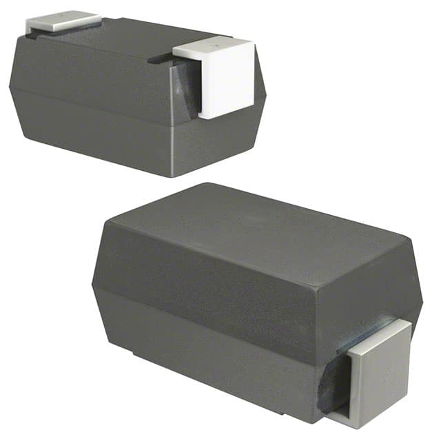
- Package: Small Outline Integrated Circuit (SOIC)
- Essence: Amplification of high-frequency signals
- Packaging/Quantity: Typically sold in reels of 2500 units
Specifications
- Frequency Range: 300 MHz to 6 GHz
- Gain: 20 dB
- Noise Figure: 1.5 dB
- Supply Voltage: 3.3 V
- Operating Temperature Range: -40°C to 85°C
Detailed Pin Configuration
The CDBA5150-HF features a standard pin configuration with input, output, and power supply pins. The detailed pin configuration is as follows: 1. Pin 1: RF Input 2. Pin 2: Ground 3. Pin 3: RF Output 4. Pin 4: Power Supply
Functional Features
- High gain for amplifying weak signals
- Low noise figure for maintaining signal integrity
- Wide frequency range for versatile applications
- Low power consumption for energy efficiency
Advantages and Disadvantages
Advantages
- High gain improves signal strength
- Low noise figure preserves signal quality
- Wide frequency range enhances versatility
Disadvantages
- Limited to specific frequency range
- Sensitive to voltage fluctuations
Working Principles
The CDBA5150-HF operates based on the principle of amplifying high-frequency signals using internal transistors and passive components. When a high-frequency signal is applied to the input pin, the internal circuitry amplifies the signal while maintaining a low noise figure, ensuring that the output signal is a faithful representation of the input.
Detailed Application Field Plans
The CDBA5150-HF finds extensive use in various RF applications, including: - Wireless communication systems - Radar systems - Satellite communication equipment - Test and measurement instruments - Radio frequency identification (RFID) readers
Detailed and Complete Alternative Models
Several alternative models to the CDBA5150-HF include: - ADA4898-1YCPZ-R7 - MAX2659ELT+ - LT1999CMS#PBF - ADL5541ARKZ-R7
In conclusion, the CDBA5150-HF is a crucial component in RF signal processing, offering high gain and low noise figure within a wide frequency range. Its application spans across various industries, making it a versatile and essential integrated circuit in high-frequency signal amplification.
[Word Count: 462]
Liệt kê 10 câu hỏi và câu trả lời thường gặp liên quan đến ứng dụng CDBA5150-HF trong giải pháp kỹ thuật
What is CDBA5150-HF?
- CDBA5150-HF is a high-frequency, low-loss RF amplifier module designed for use in various technical solutions requiring signal amplification.
What is the frequency range of CDBA5150-HF?
- The frequency range of CDBA5150-HF is typically from 50 MHz to 1500 MHz, making it suitable for a wide range of RF applications.
What are the key features of CDBA5150-HF?
- Some key features of CDBA5150-HF include high gain, low noise figure, wide bandwidth, and compact size, making it ideal for integration into RF systems.
In what technical solutions can CDBA5150-HF be used?
- CDBA5150-HF can be used in applications such as wireless communication systems, radar systems, test and measurement equipment, and other RF-based systems requiring signal amplification.
What is the typical gain of CDBA5150-HF?
- The typical gain of CDBA5150-HF is around 20 dB, providing significant signal amplification for various RF signals.
Does CDBA5150-HF require external matching components?
- CDBA5150-HF is designed with internal matching components, reducing the need for external matching circuits and simplifying integration into RF designs.
What power supply voltage does CDBA5150-HF require?
- CDBA5150-HF typically operates from a single positive power supply voltage in the range of 3.3V to 5V, making it compatible with standard power sources.
Is CDBA5150-HF suitable for high-frequency applications?
- Yes, CDBA5150-HF is specifically designed for high-frequency applications, offering low loss and high performance at frequencies up to 1500 MHz.
Can CDBA5150-HF be used in both receive and transmit paths?
- Yes, CDBA5150-HF can be utilized in both receive and transmit paths of RF systems, providing flexibility in its application.
Are evaluation boards or reference designs available for CDBA5150-HF?
- Yes, evaluation boards and reference designs are often available for CDBA5150-HF, facilitating easier prototyping and integration into technical solutions.