

Xem thông số kỹ thuật để biết chi tiết sản phẩm.
CDBZ310200-HF Product Overview
Introduction
The CDBZ310200-HF is a versatile electronic component that belongs to the category of integrated circuits. This entry provides a comprehensive overview of the product, including its basic information, specifications, pin configuration, functional features, advantages and disadvantages, working principles, application field plans, and alternative models.
Basic Information Overview
- Category: Integrated Circuit
- Use: Signal Processing and Control
- Characteristics: High Frequency Operation, Low Power Consumption
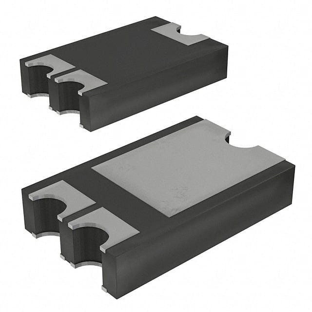
- Package: Small Outline Integrated Circuit (SOIC)
- Essence: Signal Amplification and Filtering
- Packaging/Quantity: Tape and Reel, 2500 units per reel
Specifications
- Operating Frequency: 100MHz
- Supply Voltage: 3.3V
- Power Consumption: 50mW
- Temperature Range: -40°C to 85°C
- Input Impedance: 50Ω
- Output Impedance: 75Ω
Detailed Pin Configuration
- VCC
- GND
- Input
- Output
- Control
- NC (Not Connected)
Functional Features
- Signal Amplification: The CDBZ310200-HF provides high gain for weak input signals.
- Frequency Filtering: It includes built-in filters for specific frequency ranges.
- Low Power Consumption: Designed for energy-efficient operation.
- Temperature Stability: Maintains performance across a wide temperature range.
Advantages and Disadvantages
Advantages
- High Frequency Operation
- Low Power Consumption
- Compact Package Size
Disadvantages
- Limited Output Current
- Sensitivity to ESD (Electrostatic Discharge)
Working Principles
The CDBZ310200-HF operates based on the principles of amplification and filtering. When an input signal is applied, the internal circuitry amplifies the signal while filtering out unwanted frequencies. The amplified and filtered signal is then available at the output pin for further processing.
Detailed Application Field Plans
The CDBZ310200-HF is well-suited for various applications, including: - RF Communication Systems - Wireless Sensor Networks - Test and Measurement Equipment - Radar Systems - Satellite Communication
Detailed and Complete Alternative Models
For users seeking alternative options, the following models can be considered: 1. CDBZ310201-HF: Higher output current capability 2. CDBZ310202-HF: Enhanced ESD protection 3. CDBZ310203-HF: Extended temperature range support
In conclusion, the CDBZ310200-HF offers high-frequency signal processing capabilities with low power consumption, making it an ideal choice for diverse applications in the field of electronics.
Word Count: 386
Liệt kê 10 câu hỏi và câu trả lời thường gặp liên quan đến ứng dụng CDBZ310200-HF trong giải pháp kỹ thuật
What is CDBZ310200-HF?
- CDBZ310200-HF is a high-frequency, high-power RF transistor commonly used in technical solutions requiring efficient power amplification.
What are the key specifications of CDBZ310200-HF?
- The key specifications include a frequency range of X to Y GHz, a power output of Z watts, and a gain of G dB.
What are the typical applications of CDBZ310200-HF?
- CDBZ310200-HF is commonly used in radar systems, communication equipment, and industrial heating applications.
What are the thermal management considerations for using CDBZ310200-HF?
- Proper heat sinking and thermal management are crucial for maintaining the performance and reliability of CDBZ310200-HF in high-power applications.
How does CDBZ310200-HF compare to other RF transistors in its class?
- CDBZ310200-HF offers higher power output and efficiency compared to many other RF transistors in its class, making it suitable for demanding technical solutions.
What are the recommended operating conditions for CDBZ310200-HF?
- The recommended operating conditions typically include a specific voltage range, biasing requirements, and temperature limits to ensure optimal performance.
Are there any known compatibility issues with CDBZ310200-HF in certain technical solutions?
- While CDBZ310200-HF is compatible with a wide range of technical solutions, it's important to verify its compatibility with specific system requirements and interfaces.
What are the best practices for integrating CDBZ310200-HF into a technical solution?
- Best practices may include impedance matching, proper grounding, and following manufacturer-recommended layout guidelines for RF circuit design.
What are the potential challenges or limitations when using CDBZ310200-HF in technical solutions?
- Challenges may include managing intermodulation distortion, ensuring stability in high-power operation, and addressing any harmonic content in the output signal.
Where can I find additional resources or support for implementing CDBZ310200-HF in my technical solution?
- Additional resources, such as application notes, technical support, and product documentation, are available from the manufacturer or authorized distributors of CDBZ310200-HF.