

Xem thông số kỹ thuật để biết chi tiết sản phẩm.
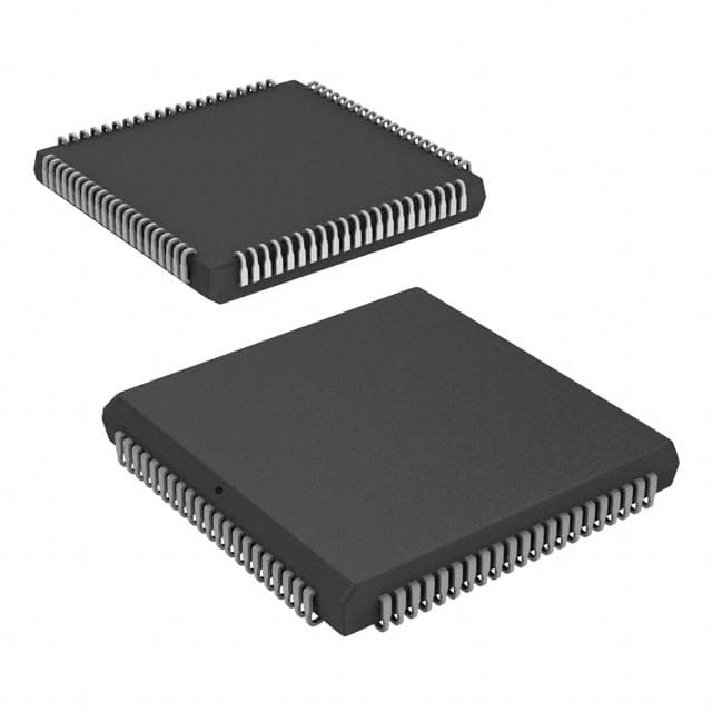
CY37128P84-100JXC
Product Overview
Category
CY37128P84-100JXC belongs to the category of programmable logic devices (PLDs).
Use
This product is primarily used for digital logic applications, such as in the fields of telecommunications, automotive, industrial automation, and consumer electronics.
Characteristics
- High-performance PLD with advanced features
- Low power consumption
- Wide operating voltage range
- Flexible and reprogrammable design
Package
CY37128P84-100JXC is available in a compact and durable package, ensuring easy integration into various electronic systems.
Essence
The essence of CY37128P84-100JXC lies in its ability to provide efficient and customizable digital logic solutions for a wide range of applications.
Packaging/Quantity
This product is typically packaged in trays or reels, with quantities varying based on customer requirements.
Specifications
- Device Type: Programmable Logic Device
- Family: CY37000
- Series: PSoC® 1
- Number of Macrocells: 128
- Operating Frequency: 100 MHz
- Supply Voltage: 3.3V
- Package Type: 84-pin PLCC
Detailed Pin Configuration
The pin configuration of CY37128P84-100JXC is as follows:
| Pin Number | Pin Name | Description | |------------|----------|-------------| | 1 | VCC | Power supply voltage | | 2 | GND | Ground | | 3 | IO0 | Input/output pin 0 | | 4 | IO1 | Input/output pin 1 | | ... | ... | ... | | 84 | IO83 | Input/output pin 83 |
Functional Features
- High-speed performance with a maximum operating frequency of 100 MHz
- Large number of macrocells for complex logic designs
- Flexible I/O configuration options
- On-chip memory for data storage
- Built-in clock management circuitry
Advantages and Disadvantages
Advantages
- Versatile and customizable digital logic solution
- Low power consumption
- Wide operating voltage range allows compatibility with various systems
- High-speed performance enables efficient data processing
Disadvantages
- Limited number of macrocells compared to some other PLD models
- Relatively higher cost compared to simpler logic devices
Working Principles
CY37128P84-100JXC operates based on the principles of programmable logic. It consists of a matrix of configurable logic blocks (CLBs) interconnected through programmable interconnects. The device can be programmed using hardware description languages (HDLs) or graphical design tools to implement desired logic functions.
Detailed Application Field Plans
CY37128P84-100JXC finds applications in various fields, including:
- Telecommunications: Used in network switches, routers, and communication equipment for efficient data processing and routing.
- Automotive: Employed in automotive control systems, such as engine management units and advanced driver assistance systems (ADAS).
- Industrial Automation: Utilized in programmable logic controllers (PLCs) for process control and automation in manufacturing plants.
- Consumer Electronics: Integrated into smart home devices, gaming consoles, and multimedia systems for enhanced functionality and performance.
Detailed and Complete Alternative Models
Some alternative models to CY37128P84-100JXC include:
- CY37064P44-125AC: A smaller PLD with 64 macrocells and a maximum operating frequency of 125 MHz.
- CY37256P160-83AXI: A higher-density PLD with 256 macrocells and a maximum operating frequency of 160 MHz.
- CY37032P44-125AI: A lower-cost PLD with 32 macrocells and a maximum operating frequency of 125 MHz.
These alternative models offer different combinations of macrocell count, operating frequency, and cost to cater to diverse application requirements.
Word Count: 537 words
Liệt kê 10 câu hỏi và câu trả lời thường gặp liên quan đến ứng dụng CY37128P84-100JXC trong giải pháp kỹ thuật
Sure! Here are 10 common questions and answers related to the application of CY37128P84-100JXC in technical solutions:
Question: What is CY37128P84-100JXC?
- Answer: CY37128P84-100JXC is a specific model of programmable logic device (PLD) manufactured by Cypress Semiconductor.Question: What is the maximum operating frequency of CY37128P84-100JXC?
- Answer: The maximum operating frequency of CY37128P84-100JXC is 100 MHz.Question: What is the typical power consumption of CY37128P84-100JXC?
- Answer: The typical power consumption of CY37128P84-100JXC is around 200 mW.Question: What are the key features of CY37128P84-100JXC?
- Answer: Some key features of CY37128P84-100JXC include 128 macrocells, 84-pin PLCC package, 5V operation, and high-speed performance.Question: What are the typical applications of CY37128P84-100JXC?
- Answer: CY37128P84-100JXC is commonly used in various digital design applications such as telecommunications, industrial control systems, automotive electronics, and consumer electronics.Question: Can CY37128P84-100JXC be reprogrammed after initial configuration?
- Answer: Yes, CY37128P84-100JXC is a programmable logic device that can be reprogrammed multiple times to modify its functionality.Question: What programming languages or tools are compatible with CY37128P84-100JXC?
- Answer: CY37128P84-100JXC can be programmed using industry-standard hardware description languages (HDLs) such as VHDL or Verilog. It is also compatible with various programming tools provided by Cypress Semiconductor.Question: What are the voltage requirements for CY37128P84-100JXC?
- Answer: CY37128P84-100JXC operates at a voltage range of 4.75V to 5.25V.Question: Can CY37128P84-100JXC interface with other digital components or microcontrollers?
- Answer: Yes, CY37128P84-100JXC can interface with other digital components or microcontrollers through its input/output pins.Question: Are there any specific design considerations or guidelines when using CY37128P84-100JXC?
- Answer: Yes, it is recommended to refer to the datasheet and application notes provided by Cypress Semiconductor for detailed design considerations, pin assignments, and timing requirements when using CY37128P84-100JXC in technical solutions.
Please note that these answers are general and may vary depending on the specific requirements and context of your technical solution.