

Xem thông số kỹ thuật để biết chi tiết sản phẩm.
Encyclopedia Entry: 74AUP1G126FZ4-7
Product Overview
- Category: Integrated Circuit (IC)
- Use: Logic Gate Buffer/Driver
- Characteristics: High-speed, low-power consumption
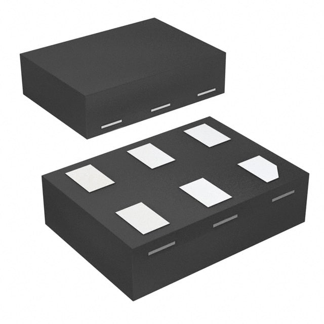
- Package: SOT-953
- Essence: Single gate buffer with tri-state output
- Packaging/Quantity: Tape and Reel, 3000 units per reel
Specifications
- Supply Voltage: 0.8V to 3.6V
- Input Voltage Range: -0.5V to VCC + 0.5V
- Output Voltage Range: GND to VCC
- Operating Temperature Range: -40°C to +125°C
- Propagation Delay: 2.9ns (typical) at 3.3V supply voltage
Detailed Pin Configuration
The 74AUP1G126FZ4-7 IC has the following pin configuration:
| Pin Number | Pin Name | Description | |------------|----------|-------------| | 1 | GND | Ground | | 2 | A | Input | | 3 | Y | Output | | 4 | OE | Output Enable | | 5 | VCC | Supply Voltage |
Functional Features
- Single gate buffer with tri-state output
- Provides buffering and driving capabilities for digital signals
- Enables or disables the output using the Output Enable (OE) pin
- Supports bidirectional communication between different logic families
- High-speed operation with low power consumption
Advantages and Disadvantages
Advantages: - Compact size and low power consumption make it suitable for portable devices - Tri-state output allows for efficient bus sharing in multi-device systems - Wide operating voltage range enables compatibility with various power supply levels
Disadvantages: - Limited output current capability may restrict its use in high-current applications - Single gate configuration limits the number of logic functions it can perform
Working Principles
The 74AUP1G126FZ4-7 is a single gate buffer with a tri-state output. It operates by receiving digital input signals through the A pin and amplifying them to provide a buffered output at the Y pin. The Output Enable (OE) pin controls the tri-state output, allowing the device to be enabled or disabled.
When the OE pin is low (logic 0), the output is active and reflects the input signal. When the OE pin is high (logic 1), the output is in a high-impedance state, effectively disconnecting it from the rest of the circuit. This tri-state feature enables efficient bus sharing in multi-device systems.
Detailed Application Field Plans
The 74AUP1G126FZ4-7 IC finds applications in various fields, including: 1. Portable electronic devices such as smartphones, tablets, and wearables. 2. Communication systems where buffering and driving of digital signals are required. 3. Industrial automation for signal conditioning and level shifting. 4. Automotive electronics for interfacing between different logic families. 5. Consumer electronics for general-purpose logic level translation.
Detailed and Complete Alternative Models
Some alternative models that offer similar functionality to the 74AUP1G126FZ4-7 IC include: - SN74LVC1G126DBVR - MC74VHC1GT126DF1G - TC7SZ126AFK(TE85L,F)
These alternatives have comparable characteristics and can be used as substitutes depending on specific requirements.
Word count: 453 words
Liệt kê 10 câu hỏi và câu trả lời thường gặp liên quan đến ứng dụng 74AUP1G126FZ4-7 trong giải pháp kỹ thuật
Sure! Here are 10 common questions and answers related to the application of 74AUP1G126FZ4-7 in technical solutions:
Q1: What is the function of the 74AUP1G126FZ4-7? A1: The 74AUP1G126FZ4-7 is a single bus buffer gate with 3-state output. It is used to control the flow of data between different parts of a circuit.
Q2: What is the operating voltage range for this device? A2: The 74AUP1G126FZ4-7 operates within a voltage range of 0.8V to 3.6V.
Q3: Can I use this device in battery-powered applications? A3: Yes, the low operating voltage range makes it suitable for battery-powered applications.
Q4: What is the maximum output current of this device? A4: The maximum output current of the 74AUP1G126FZ4-7 is typically 32mA.
Q5: Can I connect multiple devices together using this buffer gate? A5: Yes, you can connect multiple devices together by cascading them using the output and input pins.
Q6: Does this device have built-in protection features? A6: Yes, the 74AUP1G126FZ4-7 has built-in ESD (Electrostatic Discharge) protection to prevent damage from static electricity.
Q7: What is the propagation delay of this buffer gate? A7: The typical propagation delay of the 74AUP1G126FZ4-7 is around 2.5ns.
Q8: Can I use this device in high-speed applications? A8: Yes, the 74AUP1G126FZ4-7 is designed for high-speed operation and can be used in applications with fast data transfer rates.
Q9: Is this device compatible with other logic families? A9: Yes, the 74AUP1G126FZ4-7 is compatible with a wide range of logic families, including TTL, CMOS, and LVCMOS.
Q10: Can I use this buffer gate for level shifting purposes? A10: Yes, the 74AUP1G126FZ4-7 can be used for level shifting between different voltage domains within a circuit.
Please note that these answers are general and may vary depending on specific application requirements.