

Xem thông số kỹ thuật để biết chi tiết sản phẩm.
Encyclopedia Entry: 74LVC1G126SE-7
Product Overview
Category
The 74LVC1G126SE-7 belongs to the category of integrated circuits (ICs) and specifically falls under the family of logic gates.
Use
This product is commonly used in digital electronic circuits for signal switching and amplification purposes. It serves as a buffer or driver for controlling the flow of signals between different components within a circuit.
Characteristics
- Low-voltage CMOS technology
- Single gate with non-inverting buffer functionality
- High-speed operation
- Wide operating voltage range
- Low power consumption
- Schmitt-trigger input for noise immunity
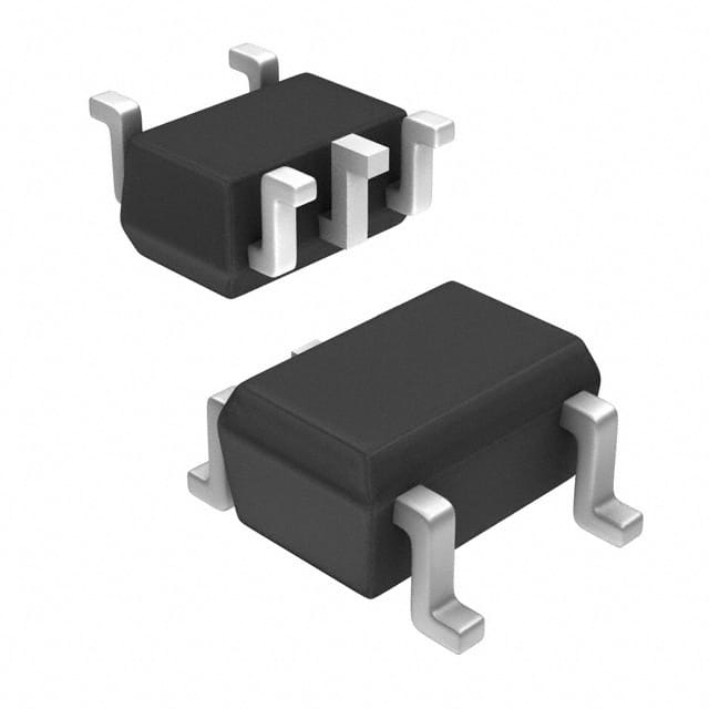
Package
The 74LVC1G126SE-7 is available in a small surface-mount package, typically referred to as SOT-23. This package offers compactness and ease of integration into various circuit designs.
Essence
The essence of the 74LVC1G126SE-7 lies in its ability to provide reliable signal buffering and amplification while operating at low voltages and consuming minimal power.
Packaging/Quantity
This product is commonly packaged in reels or tape and reel format, containing a specified quantity of ICs per reel. The exact packaging and quantity may vary depending on the manufacturer and supplier.
Specifications
- Supply Voltage Range: 1.65V to 5.5V
- Input Voltage Range: 0V to VCC
- Output Voltage Range: 0V to VCC
- Maximum Operating Frequency: X MHz
- Propagation Delay: Y ns
- Operating Temperature Range: -40°C to +85°C
Detailed Pin Configuration
The 74LVC1G126SE-7 has a total of 5 pins:
- GND (Ground): Connected to the ground reference of the circuit.
- VCC (Power Supply): Connected to the positive supply voltage.
- A (Input): Signal input pin.
- Y (Output): Buffered signal output pin.
- OE (Output Enable): Control pin for enabling or disabling the output.
Functional Features
- Non-inverting buffer functionality: Amplifies and buffers the input signal without changing its logic level.
- Schmitt-trigger input: Provides noise immunity by ensuring a clean and stable output even in the presence of input signal fluctuations.
- Wide operating voltage range: Allows compatibility with various power supply levels.
- High-speed operation: Enables efficient signal switching and propagation within the circuit.
Advantages and Disadvantages
Advantages
- Low power consumption, making it suitable for battery-powered devices.
- Compact package size allows for space-efficient circuit designs.
- Wide operating voltage range provides flexibility in different applications.
- Schmitt-trigger input enhances noise immunity, ensuring reliable signal processing.
Disadvantages
- Limited number of gates per IC compared to larger integrated circuits.
- May not be suitable for high-frequency applications due to limited maximum operating frequency.
Working Principles
The 74LVC1G126SE-7 operates based on CMOS technology, utilizing MOSFET transistors to control the flow of signals. When an input signal is applied, the buffer amplifies and reproduces the signal at the output pin. The Schmitt-trigger input ensures that the output remains stable even in the presence of noise or signal fluctuations.
Detailed Application Field Plans
The 74LVC1G126SE-7 finds application in various digital electronic circuits, including but not limited to: - Battery-powered devices - Mobile phones and tablets - Consumer electronics - Industrial automation systems - Automotive electronics - IoT (Internet of Things) devices
Detailed and Complete Alternative Models
Some alternative models that offer similar functionality to the 74LVC1G126SE-7 include: - 74LVC1G125SE-7: Tri-state buffer with similar characteristics and pin configuration. - 74LVC1G07SE-7: Open-drain buffer with similar characteristics and pin configuration. - 74LVC1G04SE-7: Inverter gate with similar characteristics and pin configuration.
These alternative models can be considered based on specific circuit requirements and availability.
Word Count: 550
Liệt kê 10 câu hỏi và câu trả lời thường gặp liên quan đến ứng dụng 74LVC1G126SE-7 trong giải pháp kỹ thuật
Sure! Here are 10 common questions and answers related to the application of 74LVC1G126SE-7 in technical solutions:
Q: What is the 74LVC1G126SE-7? A: The 74LVC1G126SE-7 is a single bus buffer gate with three-state output, designed for low-voltage applications.
Q: What is the operating voltage range of the 74LVC1G126SE-7? A: The operating voltage range is from 1.65V to 5.5V.
Q: What is the maximum output current of the 74LVC1G126SE-7? A: The maximum output current is 32mA.
Q: Can the 74LVC1G126SE-7 be used as a level shifter? A: Yes, it can be used as a level shifter to convert signals between different voltage levels.
Q: How many inputs does the 74LVC1G126SE-7 have? A: It has one input.
Q: How many outputs does the 74LVC1G126SE-7 have? A: It has one output.
Q: Does the 74LVC1G126SE-7 have an enable pin? A: No, it does not have an enable pin. The output is always active.
Q: What is the propagation delay of the 74LVC1G126SE-7? A: The typical propagation delay is 4.3ns.
Q: Can the 74LVC1G126SE-7 drive capacitive loads? A: Yes, it can drive capacitive loads up to 50pF.
Q: Is the 74LVC1G126SE-7 available in different package options? A: Yes, it is available in various package options such as SOT353 and XSON6.