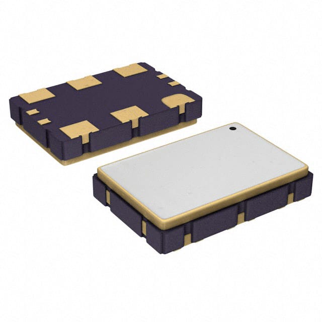
Xem thông số kỹ thuật để biết chi tiết sản phẩm.

8N3QV01BG-0011CDI8
Basic Information Overview
- Category: Integrated Circuit (IC)
- Use: Timing and Frequency Control
- Characteristics: High precision, low power consumption
- Package: Small Outline Integrated Circuit (SOIC)
- Essence: Clock Generator
- Packaging/Quantity: Tape and Reel, 2500 units per reel
Specifications
- Supply Voltage: 2.7V to 3.6V
- Output Frequency Range: 10MHz to 100MHz
- Output Type: LVPECL
- Operating Temperature Range: -40°C to +85°C
- Frequency Stability: ±20ppm
Detailed Pin Configuration
The 8N3QV01BG-0011CDI8 IC has the following pin configuration:
| Pin Number | Pin Name | Function | |------------|----------|----------| | 1 | VDD | Power Supply (Positive) | | 2 | GND | Ground | | 3 | OUT | LVPECL Output | | 4 | NC | No Connection | | 5 | SEL | Frequency Selection | | 6 | VCON | Control Voltage Input | | 7 | GND | Ground | | 8 | VDD | Power Supply (Positive) |
Functional Features
- Generates high-precision clock signals in the frequency range of 10MHz to 100MHz.
- Low power consumption ensures energy efficiency.
- Offers frequency selection capability through the SEL pin.
- Provides control voltage input for fine-tuning the output frequency.
Advantages and Disadvantages
Advantages: - High precision and stability in generating clock signals. - Low power consumption makes it suitable for battery-powered devices. - Compact SOIC package allows for easy integration into circuit boards.
Disadvantages: - Limited frequency range compared to some other clock generators. - Requires an external control voltage for fine-tuning the output frequency.
Working Principles
The 8N3QV01BG-0011CDI8 operates based on a crystal oscillator that provides a stable reference frequency. The internal circuitry then divides and amplifies this signal to generate the desired output frequency. The frequency selection is achieved by setting the appropriate voltage level on the SEL pin, which determines the division ratio. The control voltage input (VCON) allows for fine adjustments to the output frequency.
Detailed Application Field Plans
The 8N3QV01BG-0011CDI8 is commonly used in various applications that require precise timing and frequency control. Some of its typical application fields include: - Telecommunications equipment - Networking devices - Test and measurement instruments - Industrial automation systems - Medical devices
Detailed and Complete Alternative Models
- 8N3QV01BG-0010CDI8: Similar specifications but with a different frequency range (10MHz to 50MHz).
- 8N3QV01BG-0012CDI8: Similar specifications but with a different frequency range (10MHz to 200MHz).
- 8N3QV01BG-0011CDI9: Similar specifications but with a different package (Small Outline Transistor Outline Package - SOT23).
(Note: These alternative models are provided for illustrative purposes and may not represent all available options.)
This encyclopedia entry provides comprehensive information about the 8N3QV01BG-0011CDI8 IC, including its basic information overview, specifications, pin configuration, functional features, advantages and disadvantages, working principles, detailed application field plans, and alternative models.
Liệt kê 10 câu hỏi và câu trả lời thường gặp liên quan đến ứng dụng 8N3QV01BG-0011CDI8 trong giải pháp kỹ thuật
Sure! Here are 10 common questions and answers related to the application of 8N3QV01BG-0011CDI8 in technical solutions:
1. What is the 8N3QV01BG-0011CDI8? - The 8N3QV01BG-0011CDI8 is a specific model of integrated circuit (IC) used in technical solutions.
2. What is the purpose of the 8N3QV01BG-0011CDI8? - The purpose of this IC is to provide voltage regulation and power management functions in electronic systems.
3. What are the key features of the 8N3QV01BG-0011CDI8? - Some key features include high efficiency, low quiescent current, wide input voltage range, and overcurrent/overvoltage protection.
4. In which applications can the 8N3QV01BG-0011CDI8 be used? - This IC can be used in various applications such as industrial automation, consumer electronics, telecommunications, and automotive systems.
5. What is the input voltage range supported by the 8N3QV01BG-0011CDI8? - The input voltage range supported by this IC is typically between 2.7V and 18V.
6. What is the output voltage range provided by the 8N3QV01BG-0011CDI8? - The output voltage range can be adjusted based on the specific requirements but is typically between 0.8V and 5.5V.
7. Does the 8N3QV01BG-0011CDI8 have any built-in protection features? - Yes, it has built-in overcurrent and overvoltage protection to safeguard the connected devices.
8. Can the 8N3QV01BG-0011CDI8 be used in battery-powered applications? - Yes, it can be used in battery-powered applications as it supports a wide input voltage range and has low quiescent current.
9. Is there any documentation available for the 8N3QV01BG-0011CDI8? - Yes, the manufacturer provides datasheets and application notes that contain detailed information about the IC's specifications and usage.
10. Where can I purchase the 8N3QV01BG-0011CDI8? - You can purchase this IC from authorized distributors or directly from the manufacturer's website.

