

Xem thông số kỹ thuật để biết chi tiết sản phẩm.
8T49N004A-000NLGI
Overview
Category
The 8T49N004A-000NLGI belongs to the category of electronic components.
Use
This product is commonly used in electronic devices for various applications.
Characteristics
- High precision and accuracy
- Wide operating temperature range
- Low power consumption
- Compact size
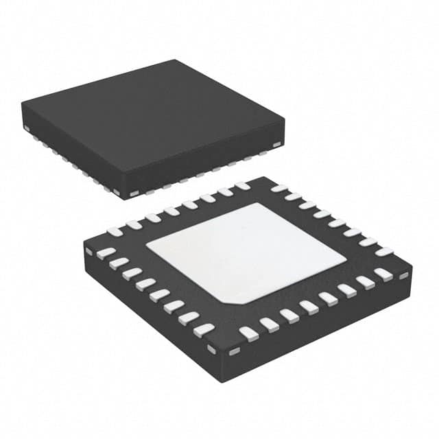
Package
The 8T49N004A-000NLGI comes in a standard package suitable for electronic component installation.
Essence
The essence of this product lies in its ability to provide precise timing and synchronization functions in electronic systems.
Packaging/Quantity
Each package of 8T49N004A-000NLGI contains a single unit of the product.
Specifications and Parameters
- Model: 8T49N004A-000NLGI
- Operating Temperature Range: -40°C to +85°C
- Supply Voltage: 3.3V
- Frequency Range: 1 MHz to 200 MHz
- Output Type: LVCMOS, LVDS, HCSL
- Package Type: QFN
Detailed Pin Configuration
The pin configuration of 8T49N004A-000NLGI is as follows:
| Pin Number | Pin Name | Description | |------------|----------|-------------| | 1 | VDD | Power supply voltage input | | 2 | GND | Ground | | 3 | OUT0 | Output 0 | | 4 | OUT1 | Output 1 | | 5 | OUT2 | Output 2 | | 6 | OUT3 | Output 3 | | 7 | REFCLK | Reference clock input | | 8 | XTAL | Crystal oscillator input | | 9 | SDA | I2C data input/output | | 10 | SCL | I2C clock input |
Functional Characteristics
The 8T49N004A-000NLGI offers the following functional characteristics:
- Clock generation and distribution
- Frequency multiplication and division
- Phase-locked loop (PLL) operation
- Programmable output formats
- I2C interface for configuration
Advantages and Disadvantages
Advantages
- High precision timing capabilities
- Wide frequency range
- Flexible output options
- Compact size
Disadvantages
- Requires external crystal oscillator for reference clock input
- Limited to specific supply voltage range
Applicable Range of Products
The 8T49N004A-000NLGI is applicable in a wide range of electronic devices, including but not limited to:
- Communication equipment
- Consumer electronics
- Industrial automation systems
- Automotive electronics
- Medical devices
Working Principles
The working principle of 8T49N004A-000NLGI involves generating and distributing precise clock signals using a PLL circuit. The reference clock input is used to synchronize the internal oscillator, which then generates the desired output frequencies based on user configuration.
Detailed Application Field Plans
The 8T49N004A-000NLGI can be applied in various fields, such as:
- Telecommunications: Providing accurate timing for network synchronization.
- Data centers: Synchronizing server clusters and storage systems.
- Automotive: Timing and synchronization for vehicle control systems.
- Industrial automation: Coordination of distributed control systems.
- Medical devices: Precise timing for medical imaging and diagnostic equipment.
Detailed Alternative Models
Some alternative models to consider are:
- 8T49N002A-000NLGI
- 8T49N003A-000NLGI
- 8T49N005A-000NLGI
- 8T49N006A-000NLGI
- 8T49N007A-000NLGI
5 Common Technical Questions and Answers
Q: What is the maximum frequency range supported by 8T49N004A-000NLGI? A: The product supports a frequency range of 1 MHz to 200 MHz.
Q: Can I use this product in automotive applications? A: Yes, the 8T49N004A-000NLGI is suitable for automotive electronics.
Q: Does it require an external power supply? A: Yes, the product requires a 3.3V power supply.
Q: What are the available output types? A: The 8T49N004A-000NLGI supports LVCMOS, LVDS, and HCSL output types.
Q: Is the pin configuration compatible with standard QFN packages? A: Yes, the pin configuration follows the standard QFN package layout.
This concludes the encyclopedia entry for 8T49N004A