

Xem thông số kỹ thuật để biết chi tiết sản phẩm.
8T49N286A-993NLGI
Product Overview
Category
The 8T49N286A-993NLGI belongs to the category of electronic components.
Use
This product is commonly used in electronic devices for various applications, including telecommunications, consumer electronics, and industrial equipment.
Characteristics
- High precision and accuracy
- Low power consumption
- Wide operating temperature range
- Compact size
- Easy integration into existing systems
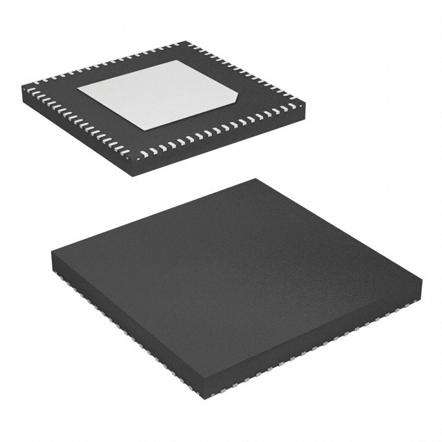
Package
The 8T49N286A-993NLGI is available in a small surface-mount package, which allows for easy installation on printed circuit boards (PCBs).
Essence
This product serves as a timing device, providing precise clock signals to synchronize the operation of different components within an electronic system.
Packaging/Quantity
The 8T49N286A-993NLGI is typically packaged in reels or trays, with a quantity of 1000 units per reel/tray.
Specifications
- Frequency range: 1 Hz to 500 MHz
- Supply voltage: 2.5 V to 3.3 V
- Output type: LVCMOS
- Operating temperature range: -40°C to +85°C
- Phase noise: -120 dBc/Hz at 10 kHz offset
Detailed Pin Configuration
The 8T49N286A-993NLGI has a total of 16 pins, each serving a specific function within the device. The pin configuration is as follows:
- VDD: Power supply input
- GND: Ground connection
- OUT0: Clock output 0
- OUT1: Clock output 1
- OUT2: Clock output 2
- OUT3: Clock output 3
- OUT4: Clock output 4
- OUT5: Clock output 5
- OUT6: Clock output 6
- OUT7: Clock output 7
- OUT8: Clock output 8
- OUT9: Clock output 9
- OUT10: Clock output 10
- OUT11: Clock output 11
- OUT12: Clock output 12
- OUT13: Clock output 13
Functional Features
- Frequency synthesis and multiplication
- Phase-locked loop (PLL) operation
- Programmable output frequencies
- Spread spectrum modulation support
- Jitter attenuation capabilities
Advantages and Disadvantages
Advantages
- High precision and accuracy ensure reliable timing synchronization.
- Low power consumption contributes to energy-efficient designs.
- Wide operating temperature range allows for use in various environments.
- Compact size enables integration into space-constrained systems.
- Easy integration simplifies the design and manufacturing process.
Disadvantages
- Limited frequency range compared to some other timing devices.
- Higher cost compared to less precise alternatives.
- Requires careful consideration of PCB layout and signal integrity.
Working Principles
The 8T49N286A-993NLGI operates based on a PLL architecture, where an input reference clock is multiplied and synthesized to generate multiple output clocks with programmable frequencies. The PLL circuitry ensures that the output clocks are phase-locked and synchronized to the input reference, providing accurate timing signals for the system.
Detailed Application Field Plans
The 8T49N286A-993NLGI finds applications in various fields, including:
- Telecommunications: Used in network equipment, routers, and switches to synchronize data transmission and reception.
- Consumer Electronics: Integrated into smartphones, tablets, and multimedia devices to ensure proper timing for audio/video processing and communication interfaces.
- Industrial Equipment: Employed in automation systems, control panels, and sensors to maintain precise timing for synchronized operations.
Detailed and Complete Alternative Models
- 8T49N286A-994NLGI: Similar to the 8T49N286A-993NLGI, but with extended frequency range up to 1 GHz.
- 8T49N286B-993NLGI: Offers additional features such as integrated voltage-controlled oscillator (VCO) and frequency modulation capabilities.
- 8T49N286C-993NLGI: Provides enhanced jitter attenuation performance for applications requiring ultra-low phase noise.
These alternative models offer different specifications and features to cater to specific requirements in various applications.
In conclusion, the 8T49N286A-993NLGI is a versatile timing device that provides precise clock signals for electronic systems. Its high precision, low power consumption, and compact size make it suitable for a wide range of applications. However, designers should consider its limited frequency range and higher cost compared to alternatives.
Liệt kê 10 câu hỏi và câu trả lời thường gặp liên quan đến ứng dụng 8T49N286A-993NLGI trong giải pháp kỹ thuật
Sure! Here are 10 common questions and answers related to the application of 8T49N286A-993NLGI in technical solutions:
Question: What is the purpose of the 8T49N286A-993NLGI in technical solutions?
Answer: The 8T49N286A-993NLGI is a clock generator and jitter attenuator IC used to generate precise clock signals in various technical applications.Question: What is the input voltage range for the 8T49N286A-993NLGI?
Answer: The input voltage range for this IC is typically between 1.8V and 3.3V.Question: Can the 8T49N286A-993NLGI be used in high-speed data communication systems?
Answer: Yes, it can be used in high-speed data communication systems as it supports various protocols like Ethernet, PCIe, SATA, USB, etc.Question: How many output channels does the 8T49N286A-993NLGI have?
Answer: This IC has six differential output channels, which can be configured to provide different clock frequencies.Question: Does the 8T49N286A-993NLGI support frequency margining?
Answer: Yes, it supports frequency margining, allowing users to adjust the output frequency within a specified range.Question: Can the 8T49N286A-993NLGI synchronize with an external reference clock?
Answer: Yes, it can synchronize with an external reference clock to ensure accurate timing across multiple devices.Question: What is the typical phase noise performance of the 8T49N286A-993NLGI?
Answer: The phase noise performance is typically -150 dBc/Hz at 100 kHz offset, making it suitable for applications with stringent timing requirements.Question: Does the 8T49N286A-993NLGI have programmable output voltage levels?
Answer: Yes, it has programmable output voltage levels to match the requirements of different devices or systems.Question: Can the 8T49N286A-993NLGI be used in automotive applications?
Answer: Yes, it is designed to meet the stringent requirements of automotive applications, including AEC-Q100 qualification.Question: What is the package type for the 8T49N286A-993NLGI?
Answer: It is available in a small-footprint 32-pin QFN package, which is suitable for space-constrained designs.
Please note that these answers are general and may vary depending on the specific application and requirements.