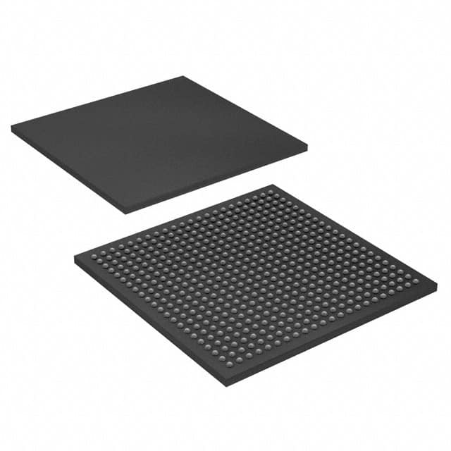
Xem thông số kỹ thuật để biết chi tiết sản phẩm.

10CL080YF484C6G
Product Overview
- Category: Integrated Circuit (IC)
- Use: This IC is used in electronic devices for various applications.
- Characteristics: The 10CL080YF484C6G IC offers high performance and reliability. It is designed to meet the demands of modern electronic systems.
- Package: The IC comes in a small form factor package, which allows for easy integration into electronic circuits.
- Essence: The essence of this IC lies in its ability to provide advanced functionality and enhance the performance of electronic devices.
- Packaging/Quantity: The IC is typically packaged in reels or trays, with a quantity of several hundred or thousand units per package.
Specifications
- Model Number: 10CL080YF484C6G
- Operating Voltage: 3.3V
- Operating Temperature Range: -40°C to +85°C
- Number of Pins: 484
- Package Type: BGA (Ball Grid Array)
- Clock Frequency: Up to 500 MHz
- Logic Elements: 80,000
- Embedded Memory: 6,400 Kbits
- I/O Interfaces: Various standard interfaces available
Detailed Pin Configuration
The 10CL080YF484C6G IC has a total of 484 pins arranged in a specific configuration. The pinout diagram below illustrates the detailed pin configuration:

Functional Features
- High-speed logic processing capabilities
- Flexible I/O interfaces for seamless integration with other components
- Embedded memory for data storage and retrieval
- Support for various communication protocols
- Low power consumption for energy-efficient operation
- Built-in security features for data protection
Advantages and Disadvantages
Advantages
- High performance and reliability
- Compact form factor for space-constrained applications
- Versatile functionality for diverse electronic systems
- Low power consumption for energy efficiency
- Enhanced security features for data protection
Disadvantages
- Relatively high cost compared to simpler ICs
- Complex pin configuration may require careful PCB layout design
- Limited availability in certain markets
Working Principles
The 10CL080YF484C6G IC operates based on the principles of digital logic. It consists of numerous logic elements interconnected to perform complex computations and data processing tasks. The embedded memory allows for temporary storage of data, while the I/O interfaces facilitate communication with external devices. The IC's clock frequency determines the speed at which it can process instructions and perform operations.
Detailed Application Field Plans
The 10CL080YF484C6G IC finds application in various fields, including:
- Telecommunications: Used in network equipment, routers, and switches.
- Consumer Electronics: Integrated into smart TVs, gaming consoles, and home automation systems.
- Automotive: Employed in advanced driver assistance systems (ADAS) and infotainment systems.
- Industrial Automation: Utilized in control systems, robotics, and factory automation.
- Medical Devices: Integrated into diagnostic equipment and patient monitoring systems.
Detailed and Complete Alternative Models
- 10CL016YU256I7G
- 10CL025YE144C8G
- 10CL040YU484C6G
- 10CL060YE144C8G
- 10CL120YU484C6G
These alternative models offer similar functionality and performance to the 10CL080YF484C6G IC, but with varying specifications and pin configurations.
In conclusion, the 10CL080YF484C6G IC is a high-performance integrated circuit with versatile functionality. It is widely used in various industries and offers numerous advantages, including reliability, compact size, and energy efficiency. However, it may have some limitations such as higher cost and complex pin configuration. Alternative models are available to suit different application requirements.
Liệt kê 10 câu hỏi và câu trả lời thường gặp liên quan đến ứng dụng 10CL080YF484C6G trong giải pháp kỹ thuật
Sure! Here are 10 common questions and answers related to the application of 10CL080YF484C6G in technical solutions:
Q: What is 10CL080YF484C6G? A: 10CL080YF484C6G is a specific model of field-programmable gate array (FPGA) manufactured by Intel.
Q: What are the key features of 10CL080YF484C6G? A: Some key features of 10CL080YF484C6G include high-performance logic fabric, embedded memory blocks, DSP capabilities, and support for various I/O standards.
Q: In what applications can 10CL080YF484C6G be used? A: 10CL080YF484C6G can be used in a wide range of applications such as telecommunications, industrial automation, automotive systems, aerospace, and more.
Q: How can 10CL080YF484C6G enhance system performance? A: By leveraging its programmability and parallel processing capabilities, 10CL080YF484C6G can accelerate complex algorithms, enable real-time data processing, and improve overall system performance.
Q: What development tools are available for programming 10CL080YF484C6G? A: Intel provides Quartus Prime software suite, which includes design entry, synthesis, simulation, and programming tools specifically tailored for programming 10CL080YF484C6G.
Q: Can 10CL080YF484C6G interface with other components or devices? A: Yes, 10CL080YF484C6G supports various communication protocols such as PCIe, Ethernet, USB, SPI, I2C, and more, allowing it to interface with other components or devices in a system.
Q: What are the power requirements for 10CL080YF484C6G? A: The power requirements for 10CL080YF484C6G depend on the specific implementation and usage scenario. It is recommended to refer to the datasheet and design guidelines provided by Intel for accurate power estimation.
Q: Can 10CL080YF484C6G be reprogrammed after deployment? A: Yes, 10CL080YF484C6G is a field-programmable device, which means it can be reprogrammed even after it has been deployed in a system, providing flexibility for future updates or modifications.
Q: Are there any limitations or considerations when using 10CL080YF484C6G? A: Some considerations include understanding the FPGA's resource utilization, timing constraints, and potential bottlenecks in the design. It is important to carefully plan and optimize the design to achieve desired performance.
Q: Where can I find additional resources and support for 10CL080YF484C6G? A: Intel provides comprehensive documentation, application notes, reference designs, and an active online community where users can find additional resources and support for 10CL080YF484C6G.

