

Xem thông số kỹ thuật để biết chi tiết sản phẩm.
5AGXBB1D4F35C4N
Product Overview
Category
The 5AGXBB1D4F35C4N belongs to the category of Field Programmable Gate Arrays (FPGAs).
Use
This FPGA is primarily used in electronic circuits for digital logic implementation, prototyping, and system integration.
Characteristics
- High-performance programmable logic device
- Offers flexibility and reconfigurability
- Provides high-speed data processing capabilities
- Supports complex algorithms and computations
- Enables rapid development and testing of digital designs
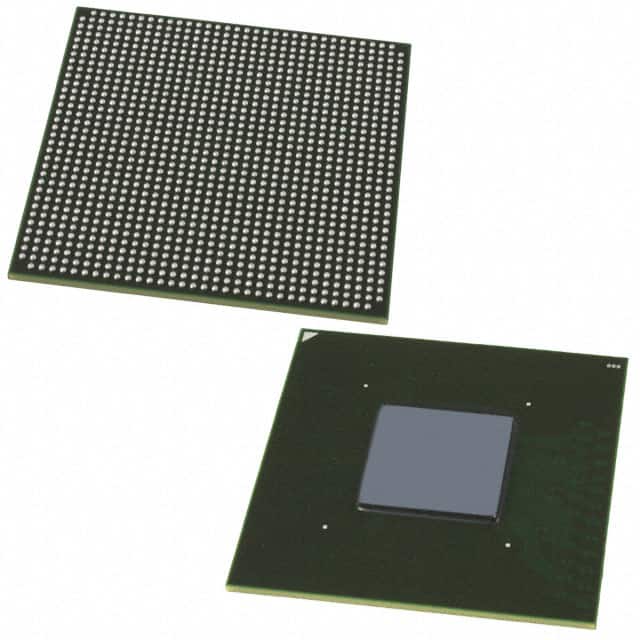
Package
The 5AGXBB1D4F35C4N comes in a compact package that ensures easy integration into electronic systems. It is designed to be mounted on a printed circuit board (PCB) using surface mount technology (SMT).
Essence
The essence of the 5AGXBB1D4F35C4N lies in its ability to provide a customizable and versatile solution for implementing digital logic functions in various applications.
Packaging/Quantity
The 5AGXBB1D4F35C4N is typically packaged in trays or reels, depending on the quantity ordered. The packaging ensures safe transportation and storage of the FPGAs.
Specifications
- Model: 5AGXBB1D4F35C4N
- Manufacturer: [Insert Manufacturer Name]
- Logic Elements: 1,400,000
- Embedded Memory: 3,888 Kbits
- Maximum Operating Frequency: 500 MHz
- Number of I/O Pins: 896
- Voltage Supply: 1.2V
- Package Type: BGA
- Temperature Range: -40°C to +100°C
Detailed Pin Configuration
The pin configuration of the 5AGXBB1D4F35C4N is as follows:
| Pin Number | Pin Name | Description | |------------|----------|-------------| | 1 | VCCINT | Internal Core Voltage Supply | | 2 | GND | Ground | | 3 | IOB0 | Input/Output Bank 0 | | 4 | IOB1 | Input/Output Bank 1 | | ... | ... | ... | | 896 | IOB_895 | Input/Output Bank 895 |
Functional Features
- High-speed data processing capabilities
- Configurable logic elements for implementing complex digital functions
- Embedded memory blocks for efficient data storage and retrieval
- Flexible I/O banks for interfacing with external devices
- Support for various communication protocols
- Built-in security features to protect intellectual property
Advantages and Disadvantages
Advantages
- Flexibility and reconfigurability allow for rapid prototyping and design iterations.
- High-performance computing capabilities enable the implementation of complex algorithms.
- Versatile I/O options facilitate integration with different electronic systems.
- Compact package size ensures easy integration into PCB designs.
Disadvantages
- Steep learning curve for beginners due to the complexity of FPGA programming.
- Higher cost compared to traditional fixed-function integrated circuits.
- Power consumption can be relatively high, especially when operating at maximum frequency.
Working Principles
The 5AGXBB1D4F35C4N operates based on the principles of configurable logic. It consists of a large number of programmable logic elements interconnected through configurable routing resources. These logic elements can be programmed to implement desired digital functions by configuring their internal connections and behavior.
The FPGA is programmed using a hardware description language (HDL) such as VHDL or Verilog. The HDL code describes the desired digital circuit functionality, which is then synthesized and mapped onto the FPGA's programmable resources. Once programmed, the FPGA can execute the desired digital logic functions.
Detailed Application Field Plans
The 5AGXBB1D4F35C4N finds applications in various fields, including:
- Telecommunications: Used for signal processing, protocol implementation, and network infrastructure.
- Aerospace and Defense: Employed in radar systems, communication equipment, and avionics.
- Industrial Automation: Utilized for control systems, motor drives, and data acquisition.
- Medical Devices: Integrated into imaging systems, patient monitoring devices, and diagnostic equipment.
- Automotive: Applied in advanced driver-assistance systems (ADAS), infotainment systems, and engine control units.
Detailed and Complete Alternative Models
- Model: [Insert Alternative Model 1]
- Manufacturer: [Insert Manufacturer Name]
- Logic Elements: [Insert Specifications]
- Embedded Memory: [Insert Specifications]
- Maximum Operating Frequency: [Insert Specifications]
- Number of I/O Pins: [Insert Specifications]
- Voltage Supply: [Insert Specifications]
- Package Type: [Insert Specifications]
- Temperature Range: [
Liệt kê 10 câu hỏi và câu trả lời thường gặp liên quan đến ứng dụng 5AGXBB1D4F35C4N trong giải pháp kỹ thuật
Sure! Here are 10 common questions and answers related to the application of 5AGXBB1D4F35C4N in technical solutions:
Q1: What is 5AGXBB1D4F35C4N? A1: 5AGXBB1D4F35C4N is a specific model of Field-Programmable Gate Array (FPGA) manufactured by Intel.
Q2: What are the key features of 5AGXBB1D4F35C4N? A2: Some key features of 5AGXBB1D4F35C4N include high-performance processing capabilities, low power consumption, large capacity for logic elements, and support for various communication protocols.
Q3: In what applications can 5AGXBB1D4F35C4N be used? A3: 5AGXBB1D4F35C4N can be used in a wide range of applications such as telecommunications, industrial automation, automotive electronics, aerospace, and defense systems.
Q4: How can 5AGXBB1D4F35C4N enhance system performance? A4: By leveraging its high-speed processing capabilities and programmability, 5AGXBB1D4F35C4N can accelerate complex algorithms, enable real-time data processing, and provide flexibility for system customization.
Q5: Can 5AGXBB1D4F35C4N be reprogrammed after deployment? A5: Yes, 5AGXBB1D4F35C4N is a field-programmable device, meaning it can be reprogrammed even after being deployed in a system, allowing for updates and modifications without hardware changes.
Q6: What development tools are available for programming 5AGXBB1D4F35C4N? A6: Intel provides Quartus Prime software, which is a comprehensive development environment for designing and programming FPGAs like 5AGXBB1D4F35C4N.
Q7: Can 5AGXBB1D4F35C4N interface with other components in a system? A7: Yes, 5AGXBB1D4F35C4N supports various communication protocols such as PCIe, Ethernet, USB, and I2C, allowing it to interface with other components in a system seamlessly.
Q8: What are the power requirements for 5AGXBB1D4F35C4N? A8: The power requirements for 5AGXBB1D4F35C4N depend on the specific implementation and usage scenario. It is recommended to refer to the datasheet and design guidelines provided by Intel.
Q9: Are there any limitations or considerations when using 5AGXBB1D4F35C4N? A9: Some considerations include understanding the FPGA's resource utilization, managing power consumption, and ensuring proper thermal management to avoid overheating.
Q10: Where can I find additional resources and support for 5AGXBB1D4F35C4N? A10: Intel's website provides documentation, application notes, reference designs, and a community forum where you can find additional resources and seek support for 5AGXBB1D4F35C4N.