

Xem thông số kỹ thuật để biết chi tiết sản phẩm.
5CGXBC9D6F27C7N
Product Overview
Category
The 5CGXBC9D6F27C7N belongs to the category of Field Programmable Gate Arrays (FPGAs).
Use
FPGAs are integrated circuits that can be programmed and reprogrammed to perform various digital functions. The 5CGXBC9D6F27C7N is specifically designed for high-performance applications that require complex logic functions.
Characteristics
- High-performance FPGA with advanced features
- Large number of programmable logic elements
- High-speed transceivers for data communication
- On-chip memory blocks for efficient data storage
- Flexible I/O interfaces for easy integration with external devices
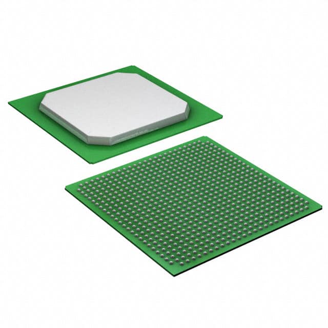
Package
The 5CGXBC9D6F27C7N comes in a compact package, suitable for surface mount technology (SMT) assembly. The package ensures proper protection and thermal dissipation for reliable operation.
Essence
The essence of the 5CGXBC9D6F27C7N lies in its ability to provide customizable digital logic functions, enabling designers to implement complex systems on a single chip.
Packaging/Quantity
The 5CGXBC9D6F27C7N is typically packaged in trays or reels, depending on the manufacturer's specifications. The quantity per package may vary, but it is commonly available in quantities of 100 or more.
Specifications
- Logic Elements: 9,600
- Embedded Memory: 1,638 Kbits
- Transceivers: 27
- Maximum Operating Frequency: 500 MHz
- I/O Pins: 622
- Voltage Range: 1.2V - 3.3V
- Package Type: BGA (Ball Grid Array)
- Package Size: 27mm x 27mm
Detailed Pin Configuration
The 5CGXBC9D6F27C7N has a complex pin configuration, with multiple pins dedicated to various functions such as input/output, power supply, clock signals, and configuration. For the detailed pin configuration, please refer to the manufacturer's datasheet.
Functional Features
- High-speed data processing capabilities
- Configurable logic elements for custom functionality
- Flexible I/O interfaces for easy integration
- On-chip memory blocks for efficient data storage
- Built-in transceivers for high-speed data communication
Advantages and Disadvantages
Advantages
- Versatile and customizable digital logic functions
- High-performance capabilities for demanding applications
- Efficient use of on-chip resources
- Easy integration with external devices
- Reconfigurable for future updates or modifications
Disadvantages
- Steep learning curve for beginners
- Higher cost compared to simpler programmable devices
- Requires specialized design tools and expertise
- Limited availability of alternative models with similar specifications
Working Principles
The 5CGXBC9D6F27C7N operates based on the principles of reconfigurable computing. It consists of an array of programmable logic elements interconnected through configurable routing resources. The device can be programmed using hardware description languages (HDL) or graphical design tools to implement desired digital logic functions. Once programmed, the FPGA executes the specified logic operations, enabling the system to perform complex tasks.
Detailed Application Field Plans
The 5CGXBC9D6F27C7N finds applications in various fields that require high-performance digital processing capabilities. Some potential application areas include:
- Telecommunications: Used in base stations, routers, and network switches for high-speed data processing and communication.
- Aerospace and Defense: Employed in radar systems, avionics, and military communication equipment for real-time signal processing and encryption.
- Industrial Automation: Integrated into control systems, robotics, and machine vision applications for precise and fast data processing.
- Medical Devices: Utilized in medical imaging, patient monitoring, and diagnostic equipment for high-speed data acquisition and analysis.
- Research and Development: Used in prototyping and testing of complex digital systems, allowing rapid iteration and design validation.
Detailed and Complete Alternative Models
While the 5CGXBC9D6F27C7N offers advanced features and performance, there are alternative FPGA models available with similar capabilities. Some notable alternatives include:
- Xilinx Virtex-7 series
- Intel Stratix 10 series
- Lattice ECP5 series
- Microsemi SmartFusion2 series
These alternative models provide a range of options to suit different application requirements, ensuring designers have flexibility in choosing the most suitable FPGA for their specific needs.
Word count: 615 words
Liệt kê 10 câu hỏi và câu trả lời thường gặp liên quan đến ứng dụng 5CGXBC9D6F27C7N trong giải pháp kỹ thuật
Sure! Here are 10 common questions and answers related to the application of 5CGXBC9D6F27C7N in technical solutions:
Q: What is the 5CGXBC9D6F27C7N? A: The 5CGXBC9D6F27C7N is a field-programmable gate array (FPGA) manufactured by Intel.
Q: What are the key features of the 5CGXBC9D6F27C7N? A: The 5CGXBC9D6F27C7N offers high-performance, low-power consumption, and a large number of programmable logic elements.
Q: In what applications can the 5CGXBC9D6F27C7N be used? A: The 5CGXBC9D6F27C7N can be used in various applications such as telecommunications, industrial automation, automotive, and aerospace.
Q: How does the 5CGXBC9D6F27C7N contribute to power efficiency? A: The 5CGXBC9D6F27C7N utilizes advanced power management techniques, allowing for efficient power usage and reducing overall energy consumption.
Q: Can the 5CGXBC9D6F27C7N support high-speed data processing? A: Yes, the 5CGXBC9D6F27C7N supports high-speed data processing with its built-in high-speed transceivers and configurable I/O standards.
Q: Is the 5CGXBC9D6F27C7N suitable for real-time signal processing applications? A: Absolutely, the 5CGXBC9D6F27C7N's high-performance capabilities make it well-suited for real-time signal processing tasks.
Q: Can the 5CGXBC9D6F27C7N be reprogrammed after deployment? A: Yes, the 5CGXBC9D6F27C7N is a field-programmable device, meaning it can be reprogrammed even after it has been deployed in a system.
Q: What development tools are available for programming the 5CGXBC9D6F27C7N? A: Intel provides Quartus Prime software, which is a comprehensive development environment for designing and programming the 5CGXBC9D6F27C7N.
Q: Are there any reference designs or application notes available for the 5CGXBC9D6F27C7N? A: Yes, Intel provides a wide range of reference designs and application notes to help users get started with implementing the 5CGXBC9D6F27C7N in their projects.
Q: Where can I find technical support for the 5CGXBC9D6F27C7N? A: Intel offers technical support through their website, where you can find documentation, forums, and contact information for further assistance.
Please note that the specific details and answers may vary depending on the manufacturer's documentation and resources available.