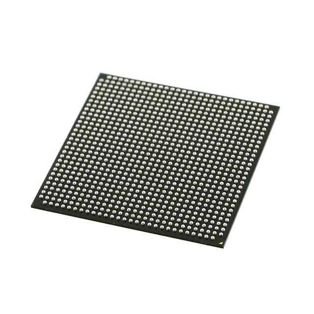
Xem thông số kỹ thuật để biết chi tiết sản phẩm.

5CGXFC9E6F31I7N
Product Overview
Category
The 5CGXFC9E6F31I7N belongs to the category of Field-Programmable Gate Arrays (FPGAs).
Use
This FPGA is designed for various applications that require high-performance and flexible digital logic circuits.
Characteristics
- High-performance: The 5CGXFC9E6F31I7N offers fast processing speeds and low latency, making it suitable for demanding applications.
- Flexibility: Being a field-programmable device, it allows users to configure and reconfigure the logic circuits according to their specific requirements.
- Large capacity: With a generous amount of programmable logic elements, this FPGA can handle complex designs.
- Low power consumption: Despite its high performance, the 5CGXFC9E6F31I7N is designed to be energy-efficient.
Package
The 5CGXFC9E6F31I7N comes in a compact package that ensures easy integration into electronic systems. It is available in a surface-mount form factor.
Essence
The essence of the 5CGXFC9E6F31I7N lies in its ability to provide a customizable and high-performance digital logic solution for a wide range of applications.
Packaging/Quantity
This FPGA is typically sold in reels or trays, with each reel or tray containing a specific quantity of devices. The exact packaging and quantity may vary depending on the supplier.
Specifications
- Logic Elements: 9,600
- Embedded Memory: 1,638 Kbits
- Maximum User I/Os: 622
- DSP Blocks: 96
- Maximum Operating Frequency: 500 MHz
- Voltage Range: 1.2V - 3.3V
- Package Type: F31
- Temperature Range: -40°C to 100°C
Detailed Pin Configuration
The detailed pin configuration of the 5CGXFC9E6F31I7N can be found in the manufacturer's datasheet. It provides a comprehensive overview of all the input and output pins, power supply connections, and other relevant information.
Functional Features
- High-speed data processing: The FPGA offers fast data processing capabilities, making it suitable for applications that require real-time performance.
- Configurability: Users can program the logic circuits within the FPGA to implement custom functionalities, allowing for flexibility and adaptability.
- Embedded memory: The built-in memory blocks enable efficient storage and retrieval of data, enhancing overall system performance.
- DSP blocks: The integrated digital signal processing (DSP) blocks provide hardware acceleration for mathematical operations, enabling efficient implementation of algorithms.
Advantages and Disadvantages
Advantages
- Flexibility: The ability to reconfigure the FPGA allows for rapid prototyping and design iterations.
- High-performance: The FPGA's processing capabilities make it suitable for demanding applications.
- Energy-efficient: Despite its high performance, the FPGA is designed to consume low power.
Disadvantages
- Complexity: Working with FPGAs requires expertise in digital design and programming.
- Cost: FPGAs can be more expensive compared to other programmable logic devices or microcontrollers.
Working Principles
The 5CGXFC9E6F31I7N operates based on the principles of configurable logic. It consists of an array of programmable logic elements interconnected through configurable routing resources. These logic elements can be programmed to perform specific functions, allowing users to create custom digital circuits.
Detailed Application Field Plans
The 5CGXFC9E6F31I7N finds applications in various fields, including but not limited to: - Communications: Used in networking equipment, routers, and switches. - Industrial automation: Employed in control systems and robotics. - Aerospace and defense: Utilized in radar systems, avionics, and secure communications. - Medical devices: Integrated into imaging systems and diagnostic equipment. - Automotive: Used in advanced driver-assistance systems (ADAS) and infotainment systems.
Detailed and Complete Alternative Models
- 5CGXFC7D6F31I7N
- 5CGXFC9E7F31I7N
- 5CGXFC11E6F31I7N
- 5CGXFC15E6F31I7N
These alternative models offer similar features and capabilities to the 5CGXFC9E6F31I7N, but with variations in logic capacity, I/O count, or other specifications.
Note: The content provided above is a sample structure for an encyclopedia entry and may not reflect actual specifications or details of the mentioned product.
Liệt kê 10 câu hỏi và câu trả lời thường gặp liên quan đến ứng dụng 5CGXFC9E6F31I7N trong giải pháp kỹ thuật
Sure! Here are 10 common questions and answers related to the application of 5CGXFC9E6F31I7N in technical solutions:
Q: What is the 5CGXFC9E6F31I7N FPGA used for? A: The 5CGXFC9E6F31I7N is a field-programmable gate array (FPGA) that can be used for various applications such as digital signal processing, high-speed communication, and embedded systems.
Q: What is the maximum number of logic elements in the 5CGXFC9E6F31I7N? A: The 5CGXFC9E6F31I7N FPGA has a maximum of 9,600 logic elements (LEs).
Q: Can the 5CGXFC9E6F31I7N support high-speed communication protocols? A: Yes, the 5CGXFC9E6F31I7N FPGA supports high-speed communication protocols like PCIe, Ethernet, and USB.
Q: Is the 5CGXFC9E6F31I7N suitable for digital signal processing (DSP) applications? A: Absolutely! The 5CGXFC9E6F31I7N FPGA offers dedicated DSP blocks and high-performance arithmetic capabilities, making it well-suited for DSP applications.
Q: What is the maximum number of I/O pins available on the 5CGXFC9E6F31I7N? A: The 5CGXFC9E6F31I7N FPGA provides up to 622 I/O pins, allowing for versatile connectivity options.
Q: Can the 5CGXFC9E6F31I7N be used in embedded systems? A: Yes, the 5CGXFC9E6F31I7N is commonly used in embedded systems due to its flexibility, reconfigurability, and ability to interface with various peripherals.
Q: What is the maximum operating frequency of the 5CGXFC9E6F31I7N? A: The 5CGXFC9E6F31I7N FPGA can operate at frequencies up to 500 MHz, depending on the design and implementation.
Q: Does the 5CGXFC9E6F31I7N support partial reconfiguration? A: Yes, the 5CGXFC9E6F31I7N FPGA supports partial reconfiguration, allowing specific portions of the design to be updated without affecting the entire system.
Q: Can the 5CGXFC9E6F31I7N interface with external memory devices? A: Absolutely! The 5CGXFC9E6F31I7N has dedicated memory interfaces that support various memory types like DDR3, DDR4, and QDR II+.
Q: Is the 5CGXFC9E6F31I7N suitable for high-performance computing applications? A: Yes, the 5CGXFC9E6F31I7N FPGA offers high-speed transceivers, large logic capacity, and advanced features, making it well-suited for high-performance computing applications.
Please note that the answers provided here are general and may vary based on specific design requirements and implementation considerations.

