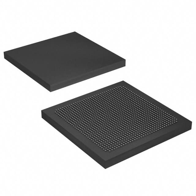
Xem thông số kỹ thuật để biết chi tiết sản phẩm.

5SGXEA7H3F35C2LN
Product Overview
Category
The 5SGXEA7H3F35C2LN belongs to the category of Field Programmable Gate Arrays (FPGAs).
Use
FPGAs are integrated circuits that can be programmed and reprogrammed to perform various digital functions. The 5SGXEA7H3F35C2LN is specifically designed for high-performance applications.
Characteristics
- High-performance FPGA with advanced features
- Large capacity and high-speed processing capabilities
- Flexible and reconfigurable design
- Low power consumption
- Suitable for complex digital designs
Package
The 5SGXEA7H3F35C2LN comes in a compact package, ensuring easy integration into electronic systems.
Essence
The essence of the 5SGXEA7H3F35C2LN lies in its ability to provide a customizable and powerful digital processing solution for a wide range of applications.
Packaging/Quantity
The 5SGXEA7H3F35C2LN is typically packaged individually and is available in various quantities depending on the requirements of the user.
Specifications
- FPGA Family: Stratix V
- Logic Elements: 352,000
- Embedded Memory: 8,062 Kbits
- DSP Blocks: 1,288
- Maximum User I/Os: 622
- Operating Voltage: 0.87V - 0.93V
- Operating Temperature: -40°C to 100°C
- Package Type: F35
- Package Pins: 896
Detailed Pin Configuration
The detailed pin configuration of the 5SGXEA7H3F35C2LN can be found in the product datasheet provided by the manufacturer. It includes information about the specific functions and connections of each pin.
Functional Features
- High-speed processing: The 5SGXEA7H3F35C2LN offers fast data processing capabilities, making it suitable for applications that require real-time performance.
- Reconfigurability: The FPGA can be reprogrammed to adapt to changing requirements or to implement different functionalities without the need for hardware changes.
- Versatility: With a large number of logic elements and embedded memory, the 5SGXEA7H3F35C2LN can handle complex digital designs and support various algorithms.
- Low power consumption: The FPGA is designed to optimize power usage, making it energy-efficient and suitable for battery-powered devices.
Advantages and Disadvantages
Advantages
- High-performance processing capabilities
- Flexibility and reconfigurability
- Large capacity for complex designs
- Low power consumption
Disadvantages
- Higher cost compared to other programmable logic devices
- Steeper learning curve for programming and design implementation
Working Principles
The 5SGXEA7H3F35C2LN operates based on the principles of digital logic. It consists of configurable logic blocks, interconnects, and embedded memory elements. The user programs the FPGA using a Hardware Description Language (HDL) to define the desired functionality. The programmed configuration is then loaded into the FPGA, allowing it to perform the specified operations.
Detailed Application Field Plans
The 5SGXEA7H3F35C2LN can be applied in various fields, including: 1. Telecommunications: Used in high-speed data transmission systems, network routers, and switches. 2. Aerospace and Defense: Employed in radar systems, avionics, and military communication equipment. 3. Industrial Automation: Utilized in control systems, robotics, and machine vision applications. 4. Medical Devices: Integrated into medical imaging systems, patient monitoring devices, and diagnostic equipment. 5. Automotive: Applied in advanced driver assistance systems (ADAS), infotainment systems, and engine control units.
Detailed and Complete Alternative Models
- 5SGXEA7H2F35C2LN: Similar to the 5SGXEA7H3F35C2LN but with a slightly lower logic element count.
- 5SGXEA7K3F35C2LN: Offers higher performance and increased logic capacity compared to the 5SGXEA7H3F35C2LN.
- 5SGXEA7N3F35C2LN: Provides enhanced power efficiency and improved signal processing capabilities.
These alternative models offer varying features and specifications, allowing users to choose the most suitable FPGA for their specific requirements.
Word count: 590 words
Liệt kê 10 câu hỏi và câu trả lời thường gặp liên quan đến ứng dụng 5SGXEA7H3F35C2LN trong giải pháp kỹ thuật
Sure! Here are 10 common questions and answers related to the application of 5SGXEA7H3F35C2LN in technical solutions:
Q: What is the 5SGXEA7H3F35C2LN FPGA used for? A: The 5SGXEA7H3F35C2LN is a Field-Programmable Gate Array (FPGA) that can be used for various applications such as high-performance computing, networking, and signal processing.
Q: What are the key features of the 5SGXEA7H3F35C2LN FPGA? A: Some key features include a high logic density, high-speed transceivers, embedded memory blocks, DSP capabilities, and support for various I/O standards.
Q: Can the 5SGXEA7H3F35C2LN FPGA be used for real-time video processing? A: Yes, the FPGA's high-performance capabilities make it suitable for real-time video processing applications like video encoding, decoding, and image recognition.
Q: How does the 5SGXEA7H3F35C2LN FPGA handle high-speed data transfer? A: The FPGA has built-in high-speed transceivers that support protocols like PCIe, Ethernet, and USB, enabling efficient data transfer at high speeds.
Q: Can the 5SGXEA7H3F35C2LN FPGA be used for implementing cryptographic algorithms? A: Absolutely, the FPGA's high logic density and embedded memory blocks make it well-suited for implementing complex cryptographic algorithms with high performance and security.
Q: Is the 5SGXEA7H3F35C2LN FPGA compatible with industry-standard development tools? A: Yes, the FPGA is compatible with popular development tools like Intel Quartus Prime, which provide a comprehensive environment for designing and programming the FPGA.
Q: Can the 5SGXEA7H3F35C2LN FPGA be used in safety-critical applications? A: Yes, the FPGA supports various safety features like error correction codes (ECC), triple modular redundancy (TMR), and partial reconfiguration, making it suitable for safety-critical applications.
Q: What kind of power requirements does the 5SGXEA7H3F35C2LN FPGA have? A: The FPGA requires a supply voltage of 1.0V for core logic and 2.5V/3.3V for I/O interfaces, with power consumption varying based on the design and utilization.
Q: Can the 5SGXEA7H3F35C2LN FPGA be used for high-performance computing applications? A: Yes, the FPGA's high logic density, embedded memory, and DSP capabilities make it suitable for accelerating computationally intensive tasks in high-performance computing applications.
Q: Are there any reference designs or application notes available for the 5SGXEA7H3F35C2LN FPGA? A: Yes, Intel provides a range of reference designs, application notes, and documentation to help users get started with the 5SGXEA7H3F35C2LN FPGA and implement various technical solutions.
Please note that the specific details and answers may vary depending on the context and requirements of the technical solution being implemented.

