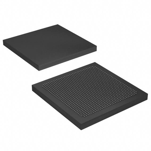
Xem thông số kỹ thuật để biết chi tiết sản phẩm.

5SGXMA7H2F35C3
Product Overview
Category
The 5SGXMA7H2F35C3 belongs to the category of Field Programmable Gate Arrays (FPGAs).
Use
This FPGA is designed for high-performance applications that require complex digital logic circuits.
Characteristics
- High-speed processing capabilities
- Configurable logic blocks
- Large number of input/output pins
- Flexible and reprogrammable design
Package
The 5SGXMA7H2F35C3 comes in a compact package, suitable for integration into various electronic systems.
Essence
The essence of this FPGA lies in its ability to provide customizable digital logic functions, enabling designers to implement complex algorithms and circuits.
Packaging/Quantity
The 5SGXMA7H2F35C3 is typically packaged individually and is available in various quantities depending on the customer's requirements.
Specifications
- FPGA Family: Stratix V
- Logic Elements: 352,000
- Embedded Memory: 8,062 Kbits
- DSP Blocks: 1,288
- Maximum User I/Os: 622
- Operating Voltage: 1.0V
- Operating Temperature: -40°C to 100°C
Detailed Pin Configuration
The pin configuration of the 5SGXMA7H2F35C3 FPGA is as follows:
- Pin 1: GND
- Pin 2: VCCIO
- Pin 3: IO_0
- Pin 4: IO_1
- ...
- Pin 622: IO_621
Functional Features
- High-speed data processing
- Configurable logic blocks for custom circuit implementation
- On-chip memory for efficient data storage
- Digital Signal Processing (DSP) blocks for signal manipulation
- Support for various communication protocols
Advantages and Disadvantages
Advantages
- Flexibility in design and reprogrammability
- High-performance capabilities
- Large number of I/O pins for versatile connectivity
- Support for complex algorithms and circuits
Disadvantages
- Higher power consumption compared to other programmable logic devices
- Steeper learning curve for beginners
- Relatively higher cost compared to simpler logic devices
Working Principles
The 5SGXMA7H2F35C3 FPGA operates based on the principles of configurable logic. It consists of a matrix of programmable logic blocks interconnected by configurable routing resources. The user can program the FPGA to implement desired digital logic functions by configuring the interconnections between logic blocks.
Detailed Application Field Plans
The 5SGXMA7H2F35C3 FPGA finds applications in various fields, including:
- Telecommunications: Used in high-speed data processing and signal manipulation in communication systems.
- Aerospace and Defense: Employed in radar systems, avionics, and secure communications.
- Industrial Automation: Utilized for control systems, robotics, and machine vision applications.
- Medical Devices: Integrated into medical imaging systems and diagnostic equipment.
- Research and Development: Used for prototyping and testing of complex digital circuits.
Detailed and Complete Alternative Models
- 5SGXEA7K2F40C2: Similar FPGA from the same family with a different configuration.
- 5SGXEB7R2F43C2: Another alternative FPGA with enhanced features and larger capacity.
- 5SGXFC7D6F31C2: FPGA with lower power consumption and reduced logic elements.
These alternative models offer varying specifications and capabilities to suit different application requirements.
Word count: 520 words
Liệt kê 10 câu hỏi và câu trả lời thường gặp liên quan đến ứng dụng 5SGXMA7H2F35C3 trong giải pháp kỹ thuật
Sure! Here are 10 common questions and answers related to the application of 5SGXMA7H2F35C3 in technical solutions:
Question: What is the 5SGXMA7H2F35C3 FPGA used for?
Answer: The 5SGXMA7H2F35C3 FPGA is commonly used for high-performance applications that require advanced processing capabilities.Question: What are some typical applications for the 5SGXMA7H2F35C3 FPGA?
Answer: Some typical applications include telecommunications, networking, industrial automation, video processing, and high-performance computing.Question: What is the maximum number of logic elements (LEs) in the 5SGXMA7H2F35C3 FPGA?
Answer: The 5SGXMA7H2F35C3 FPGA has a maximum of 622,080 LEs.Question: Can the 5SGXMA7H2F35C3 FPGA support high-speed serial interfaces?
Answer: Yes, the 5SGXMA7H2F35C3 FPGA supports various high-speed serial interfaces such as PCIe, SATA, USB, and Ethernet.Question: What is the maximum operating frequency of the 5SGXMA7H2F35C3 FPGA?
Answer: The maximum operating frequency of the 5SGXMA7H2F35C3 FPGA is dependent on the specific design and implementation, but it can reach up to several hundred megahertz or even gigahertz.Question: Does the 5SGXMA7H2F35C3 FPGA have built-in memory?
Answer: No, the 5SGXMA7H2F35C3 FPGA does not have built-in memory. However, it can be easily interfaced with external memory devices.Question: Can the 5SGXMA7H2F35C3 FPGA support multiple clock domains?
Answer: Yes, the 5SGXMA7H2F35C3 FPGA supports multiple clock domains and provides dedicated clock management resources for efficient clock domain crossing.Question: What is the power consumption of the 5SGXMA7H2F35C3 FPGA?
Answer: The power consumption of the 5SGXMA7H2F35C3 FPGA depends on the specific design and utilization. It is recommended to refer to the device datasheet for detailed power specifications.Question: Can the 5SGXMA7H2F35C3 FPGA be reprogrammed or updated after deployment?
Answer: Yes, the 5SGXMA7H2F35C3 FPGA can be reprogrammed or updated in the field using various programming methods such as JTAG, AS, or PCIe.Question: Are there any development tools available for designing with the 5SGXMA7H2F35C3 FPGA?
Answer: Yes, Intel Quartus Prime is a popular development tool that supports designing and programming the 5SGXMA7H2F35C3 FPGA, providing a comprehensive environment for FPGA development.
Please note that the answers provided here are general and may vary depending on the specific requirements and implementation of the technical solution.

