

Xem thông số kỹ thuật để biết chi tiết sản phẩm.
5SGXMABK1H40C2LN
Product Overview
Category
5SGXMABK1H40C2LN belongs to the category of Field Programmable Gate Arrays (FPGAs).
Use
FPGAs are integrated circuits that can be programmed and reprogrammed to perform various digital logic functions. They are widely used in industries such as telecommunications, automotive, aerospace, and consumer electronics.
Characteristics
- High flexibility: FPGAs can be customized to perform specific tasks by programming their internal logic.
- Parallel processing: FPGAs can execute multiple operations simultaneously, making them suitable for high-performance computing applications.
- Reconfigurability: FPGAs can be reprogrammed multiple times, allowing for easy updates and modifications.
- Low power consumption: Compared to traditional application-specific integrated circuits (ASICs), FPGAs consume less power.
Package
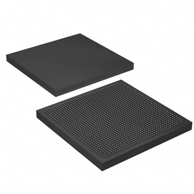
The 5SGXMABK1H40C2LN FPGA is available in a compact package, designed to be mounted on printed circuit boards (PCBs). The specific package type may vary depending on the manufacturer.
Essence
The essence of 5SGXMABK1H40C2LN lies in its ability to provide a flexible and customizable solution for digital logic implementation. It allows designers to create complex systems with reduced development time and cost.
Packaging/Quantity
The packaging and quantity of 5SGXMABK1H40C2LN depend on the manufacturer's specifications. Typically, FPGAs are supplied in trays or reels, with quantities ranging from a few units to thousands.
Specifications
- Logic elements: 40,000
- Embedded memory: 2,073,600 bits
- Maximum user I/O pins: 622
- Clock management resources: PLLs and DLLs
- Operating voltage: 1.2V
- Operating temperature range: -40°C to 100°C
- Package dimensions: Varies depending on the manufacturer
Detailed Pin Configuration
The pin configuration of 5SGXMABK1H40C2LN may vary depending on the specific package and manufacturer. It typically includes a combination of input/output pins, power supply pins, ground pins, and configuration pins. For detailed pin assignments, refer to the manufacturer's datasheet.
Functional Features
- High-speed data processing: The FPGA can handle complex algorithms and data-intensive tasks efficiently.
- Configurable I/O standards: Supports various communication protocols such as LVCMOS, LVDS, and SSTL.
- On-chip memory: Includes embedded memory blocks for storing data during operation.
- Clock management: Provides phase-locked loops (PLLs) and delay-locked loops (DLLs) for precise clock generation and synchronization.
- Built-in DSP blocks: Enables efficient implementation of digital signal processing algorithms.
Advantages and Disadvantages
Advantages
- Flexibility: FPGAs offer the ability to adapt and reconfigure hardware functionality as per the application requirements.
- Rapid prototyping: FPGAs allow quick development and testing of digital designs, reducing time-to-market.
- Cost-effective: Compared to ASICs, FPGAs have lower upfront costs and can be reprogrammed multiple times.
- Parallel processing: FPGAs excel in parallel computing applications, providing high-performance capabilities.
Disadvantages
- Power consumption: FPGAs generally consume more power compared to ASICs due to their programmable nature.
- Complexity: Designing for FPGAs requires specialized knowledge and expertise in digital logic design.
- Limited performance optimization: While FPGAs offer flexibility, they may not achieve the same level of performance as dedicated ASICs for specific tasks.
Working Principles
FPGAs consist of an array of configurable logic blocks (CLBs) interconnected through programmable routing resources. The CLBs contain look-up tables (LUTs), flip-flops, and other components that can be programmed to implement desired logic functions. The interconnections between CLBs allow data flow and communication between different parts of the FPGA.
During operation, the FPGA is configured by loading a bitstream that defines the desired logic functionality into its internal memory. This configuration process determines how the logic elements and interconnections are set up within the FPGA, enabling it to perform the desired tasks.
Detailed Application Field Plans
The 5SGXMABK1H40C2LN FPGA finds applications in various fields, including:
- Telecommunications: Used for high-speed data processing, protocol conversion, and signal modulation/demodulation.
- Automotive: Employed in advanced driver-assistance systems (ADAS), engine control units (ECUs), and infotainment systems.
- Aerospace: Utilized in avionics systems, radar signal processing, and satellite communication.
- Consumer Electronics: Found in video and audio processing devices, gaming consoles, and multimedia systems.
- Industrial Automation: Applied
Liệt kê 10 câu hỏi và câu trả lời thường gặp liên quan đến ứng dụng 5SGXMABK1H40C2LN trong giải pháp kỹ thuật
Sure! Here are 10 common questions and answers related to the application of 5SGXMABK1H40C2LN in technical solutions:
Q1: What is 5SGXMABK1H40C2LN? A1: 5SGXMABK1H40C2LN is a specific model of Field Programmable Gate Array (FPGA) manufactured by Intel.
Q2: What are the key features of 5SGXMABK1H40C2LN? A2: Some key features of 5SGXMABK1H40C2LN include high-performance processing, low power consumption, high-speed interfaces, and reprogrammability.
Q3: In what technical solutions can 5SGXMABK1H40C2LN be used? A3: 5SGXMABK1H40C2LN can be used in various technical solutions such as telecommunications, automotive systems, industrial automation, aerospace applications, and high-performance computing.
Q4: How does 5SGXMABK1H40C2LN contribute to telecommunications solutions? A4: 5SGXMABK1H40C2LN can enhance telecommunications solutions by providing high-speed data processing, efficient signal processing, and support for advanced communication protocols.
Q5: What advantages does 5SGXMABK1H40C2LN offer in automotive systems? A5: In automotive systems, 5SGXMABK1H40C2LN can enable real-time data processing, advanced driver assistance systems, improved vehicle connectivity, and enhanced safety features.
Q6: How does 5SGXMABK1H40C2LN benefit industrial automation? A6: 5SGXMABK1H40C2LN can improve industrial automation by enabling faster control loops, precise motion control, efficient data processing, and seamless integration with other industrial systems.
Q7: What role does 5SGXMABK1H40C2LN play in aerospace applications? A7: In aerospace applications, 5SGXMABK1H40C2LN can support high-performance computing, advanced navigation systems, real-time image processing, and reliable communication interfaces.
Q8: How does 5SGXMABK1H40C2LN contribute to high-performance computing? A8: 5SGXMABK1H40C2LN offers high-speed processing capabilities, parallel computing capabilities, and the ability to handle complex algorithms, making it suitable for high-performance computing applications.
Q9: Can 5SGXMABK1H40C2LN be reprogrammed? A9: Yes, 5SGXMABK1H40C2LN is a Field Programmable Gate Array (FPGA), which means it can be reprogrammed to adapt to different requirements or to fix bugs without replacing the hardware.
Q10: Are there any specific development tools or software required to work with 5SGXMABK1H40C2LN? A10: Yes, Intel provides development tools such as Quartus Prime software suite that allows users to design, simulate, and program 5SGXMABK1H40C2LN-based solutions.
Please note that the answers provided here are general and may vary depending on the specific application and requirements.