

Xem thông số kỹ thuật để biết chi tiết sản phẩm.
EP1S25F672I7
Basic Information Overview
- Category: Integrated Circuit (IC)
- Use: Programmable Logic Device (PLD)
- Characteristics: High-performance, low-power consumption
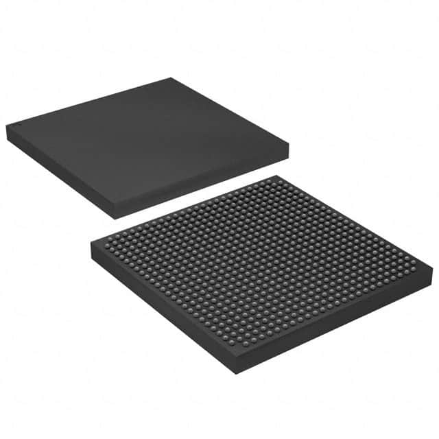
- Package: 672-pin FineLine BGA package
- Essence: FPGA (Field-Programmable Gate Array)
- Packaging/Quantity: Single unit
Specifications
- Technology: 90nm Stratix® II
- Logic Elements: 24,624
- Embedded Memory: 1,008 Kbits
- Maximum User I/Os: 622
- Operating Voltage: 1.2V
- Operating Temperature: -40°C to +100°C
- Speed Grade: 7
Detailed Pin Configuration
The EP1S25F672I7 has a total of 672 pins, each serving a specific purpose in the circuit. The pin configuration includes power supply pins, ground pins, input/output pins, clock pins, and configuration pins. A detailed pinout diagram can be found in the datasheet provided by the manufacturer.
Functional Features
- High-performance architecture allows for complex digital designs.
- Low-power consumption ensures efficient operation and reduced energy usage.
- Flexible and reprogrammable nature enables customization for various applications.
- Advanced embedded memory provides additional storage capacity.
- Support for multiple I/O standards facilitates easy integration with other devices.
Advantages and Disadvantages
Advantages: - Versatile and adaptable to different design requirements. - Offers high-speed performance for demanding applications. - Lower power consumption compared to alternative solutions. - Large number of logic elements and I/Os provide ample resources for complex designs.
Disadvantages: - Higher cost compared to traditional fixed-function integrated circuits. - Requires specialized knowledge and tools for programming and implementation. - Limited scalability beyond the available logic elements and I/Os.
Working Principles
The EP1S25F672I7 is based on FPGA technology, which allows users to configure the device according to their specific requirements. The device consists of an array of programmable logic blocks interconnected by programmable interconnects. These logic blocks can be configured to perform various functions, such as arithmetic operations, data storage, and signal processing. The interconnects enable communication between different logic blocks, allowing for the creation of complex digital circuits.
Detailed Application Field Plans
The EP1S25F672I7 finds applications in a wide range of fields, including: - Telecommunications: Used in network infrastructure equipment, routers, and switches. - Industrial Automation: Employed in control systems, robotics, and process automation. - Automotive: Integrated into advanced driver-assistance systems (ADAS) and infotainment systems. - Aerospace and Defense: Utilized in radar systems, avionics, and secure communications. - Consumer Electronics: Found in high-end audio/video equipment, gaming consoles, and smart devices.
Detailed and Complete Alternative Models
- EP1S10F484C7: Smaller version with 10,320 logic elements and 484 pins.
- EP1S40F780C6: Larger version with 39,600 logic elements and 780 pins.
- EP1S80F1508C7: Higher-end model with 79,040 logic elements and 1,508 pins.
- EP1S160F1020C6: High-capacity variant with 159,840 logic elements and 1,020 pins.
These alternative models offer varying levels of logic capacity and pin count, providing options for different design requirements.
Word Count: 346 words
Liệt kê 10 câu hỏi và câu trả lời thường gặp liên quan đến ứng dụng EP1S25F672I7 trong giải pháp kỹ thuật
Sure! Here are 10 common questions and answers related to the application of EP1S25F672I7 in technical solutions:
Q1: What is EP1S25F672I7? A1: EP1S25F672I7 is a specific model of Field-Programmable Gate Array (FPGA) manufactured by Intel.
Q2: What are the key features of EP1S25F672I7? A2: EP1S25F672I7 offers high-performance logic, embedded memory blocks, digital signal processing capabilities, and various I/O interfaces.
Q3: What are some typical applications of EP1S25F672I7? A3: EP1S25F672I7 can be used in a wide range of applications such as telecommunications, industrial automation, aerospace, automotive, and medical devices.
Q4: How does EP1S25F672I7 differ from other FPGAs? A4: EP1S25F672I7 stands out with its specific combination of performance, power efficiency, and integrated features that make it suitable for demanding applications.
Q5: What programming languages can be used with EP1S25F672I7? A5: EP1S25F672I7 can be programmed using Hardware Description Languages (HDLs) like VHDL or Verilog.
Q6: Can EP1S25F672I7 be reprogrammed after deployment? A6: Yes, EP1S25F672I7 is a reprogrammable FPGA, allowing for flexibility and updates even after deployment.
Q7: What tools are available for designing with EP1S25F672I7? A7: Intel provides design software like Quartus Prime, which includes tools for synthesis, simulation, and programming of EP1S25F672I7.
Q8: What are the power requirements for EP1S25F672I7? A8: The power requirements of EP1S25F672I7 depend on the specific design and usage scenario. It is recommended to refer to the datasheet and design guidelines provided by Intel.
Q9: Can EP1S25F672I7 interface with other components or devices? A9: Yes, EP1S25F672I7 supports various I/O standards and interfaces like PCIe, Ethernet, USB, SPI, I2C, and more, enabling seamless integration with other components or devices.
Q10: Are there any development boards available for EP1S25F672I7? A10: Yes, Intel offers development boards specifically designed for EP1S25F672I7, providing a platform for prototyping and testing designs before deployment.
Please note that the answers provided here are general and may vary depending on the specific requirements and documentation provided by Intel for EP1S25F672I7.