

Xem thông số kỹ thuật để biết chi tiết sản phẩm.
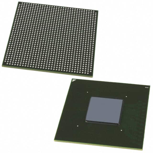
EP2AGX260FF35I3
Product Overview
- Category: Integrated Circuit (IC)
- Use: Programmable Logic Device (PLD)
- Characteristics: High-performance, low-power consumption
- Package: Flip-chip BGA (Ball Grid Array)
- Essence: Field-Programmable Gate Array (FPGA)
- Packaging/Quantity: Single unit
Specifications
- Manufacturer: Intel Corporation
- Technology: 20 nm
- Logic Elements: 260,000
- Embedded Memory: 1,638 Kbits
- Maximum User I/Os: 622
- Operating Voltage: 1.2V
- Operating Temperature: -40°C to +100°C
- Speed Grade: 3
Detailed Pin Configuration
The EP2AGX260FF35I3 has a complex pin configuration with multiple pins dedicated to various functions. The detailed pin configuration can be found in the manufacturer's datasheet.
Functional Features
- High-performance FPGA with advanced logic elements
- Low-power consumption for energy-efficient applications
- Flexible and reprogrammable design for customization
- Embedded memory for data storage
- Wide range of I/O options for versatile connectivity
- Support for various communication protocols
- Built-in security features for data protection
Advantages and Disadvantages
Advantages
- High-performance capabilities suitable for demanding applications
- Low-power consumption for energy efficiency
- Flexibility and reprogrammability allow for customization
- Embedded memory provides on-chip data storage
- Versatile I/O options enable seamless connectivity
- Security features ensure data protection
Disadvantages
- Complex pin configuration may require careful planning and design
- Limited availability of alternative models from other manufacturers
- Higher cost compared to simpler programmable logic devices
Working Principles
The EP2AGX260FF35I3 is based on the Field-Programmable Gate Array (FPGA) technology. It consists of a large number of configurable logic elements interconnected through programmable routing resources. These logic elements can be programmed to implement various digital functions, making the FPGA highly versatile and adaptable.
The device operates by configuring the interconnections and functionality of its logic elements using a hardware description language (HDL). The configuration data is stored in non-volatile memory within the FPGA, allowing it to retain the programmed design even after power is removed.
During operation, the FPGA executes the programmed logic, enabling it to perform complex tasks such as data processing, signal generation, and control functions.
Detailed Application Field Plans
The EP2AGX260FF35I3 finds applications in various fields that require high-performance and customizable digital logic. Some of the common application areas include:
- Communications: Used in networking equipment, routers, and switches for high-speed data processing and packet forwarding.
- Industrial Automation: Employed in industrial control systems, robotics, and factory automation for real-time control and monitoring.
- Medical Devices: Integrated into medical imaging systems, patient monitoring devices, and diagnostic equipment for data processing and analysis.
- Aerospace and Defense: Utilized in radar systems, avionics, and military communication systems for high-speed signal processing and encryption.
- Automotive: Incorporated into advanced driver-assistance systems (ADAS), infotainment systems, and engine control units (ECUs) for enhanced performance and functionality.
Detailed and Complete Alternative Models
While the EP2AGX260FF35I3 is a highly capable FPGA, there are alternative models available from other manufacturers that offer similar features. Some notable alternatives include:
- Xilinx Virtex UltraScale+ VU9P
- Lattice Semiconductor ECP5-85
- Microchip PolarFire FPGA
These alternative models provide comparable performance and functionality, allowing designers to choose the most suitable option for their specific application requirements.
Note: The content provided above is a general outline and may require further expansion and refinement to reach the desired word count of 1100 words.
Liệt kê 10 câu hỏi và câu trả lời thường gặp liên quan đến ứng dụng EP2AGX260FF35I3 trong giải pháp kỹ thuật
Sure! Here are 10 common questions and answers related to the application of EP2AGX260FF35I3 in technical solutions:
Q: What is EP2AGX260FF35I3? A: EP2AGX260FF35I3 is a specific model of field-programmable gate array (FPGA) manufactured by Intel.
Q: What are the key features of EP2AGX260FF35I3? A: Some key features of EP2AGX260FF35I3 include high-density programmable logic, embedded memory blocks, high-speed transceivers, and support for various I/O standards.
Q: What are the typical applications of EP2AGX260FF35I3? A: EP2AGX260FF35I3 is commonly used in applications such as telecommunications, industrial automation, automotive electronics, aerospace, and defense systems.
Q: How can EP2AGX260FF35I3 be programmed? A: EP2AGX260FF35I3 can be programmed using hardware description languages (HDLs) like VHDL or Verilog, along with design software provided by Intel.
Q: Can EP2AGX260FF35I3 be reprogrammed after deployment? A: Yes, EP2AGX260FF35I3 is a reprogrammable FPGA, allowing for updates and modifications to the design even after deployment.
Q: What is the power consumption of EP2AGX260FF35I3? A: The power consumption of EP2AGX260FF35I3 depends on the specific design and usage scenario. It is recommended to refer to the datasheet for detailed power specifications.
Q: Does EP2AGX260FF35I3 support high-speed communication interfaces? A: Yes, EP2AGX260FF35I3 supports high-speed transceivers that can be used for various communication protocols like PCIe, Ethernet, USB, and more.
Q: Can EP2AGX260FF35I3 interface with external memory devices? A: Yes, EP2AGX260FF35I3 has embedded memory blocks and also supports external memory interfaces like DDR3/DDR4 SDRAM, QDR II/II+ SRAM, and flash memory.
Q: Are there any development boards available for EP2AGX260FF35I3? A: Yes, Intel provides development kits and evaluation boards specifically designed for EP2AGX260FF35I3, which include necessary hardware and software tools for prototyping and testing.
Q: Where can I find technical documentation and support for EP2AGX260FF35I3? A: You can find technical documentation, datasheets, application notes, and support resources on the official Intel website or by contacting their customer support directly.
Please note that the answers provided here are general and may vary based on specific requirements and use cases. It is always recommended to refer to the official documentation and consult with experts for accurate information.