

Xem thông số kỹ thuật để biết chi tiết sản phẩm.
EP2C70F672C6N
Product Overview
- Category: Integrated Circuit (IC)
- Use: Programmable Logic Device (PLD)
- Characteristics: High-performance, low-power consumption
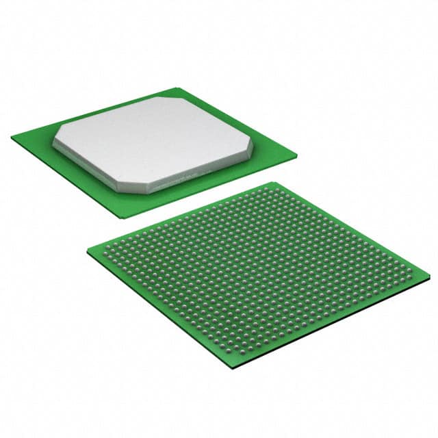
- Package: 672-ball FineLine BGA package
- Essence: Field-Programmable Gate Array (FPGA)
- Packaging/Quantity: Single unit
Specifications
- Manufacturer: Intel Corporation
- Family: Cyclone II
- Device Type: FPGA
- Number of Logic Elements: 70,208
- Number of I/O Pins: 622
- Operating Voltage: 1.2V
- Speed Grade: -6
- Maximum Frequency: 400 MHz
- Embedded Memory: 4,608 Kbits
- Total RAM Bits: 3,145,728
- Total DSP Blocks: 288
- Total PLLs: 4
Detailed Pin Configuration
The EP2C70F672C6N has a total of 672 pins. The pin configuration is as follows:
- Pin 1: VCCIO
- Pin 2: GND
- Pin 3: GND
- ...
- Pin 671: IOL1PC15_14
- Pin 672: IOL1NC15_14
For the complete pin configuration, please refer to the manufacturer's datasheet.
Functional Features
- High logic density and performance
- Low power consumption
- Flexible and reprogrammable design
- Support for various communication protocols
- On-chip memory and DSP blocks for efficient processing
- Built-in PLLs for clock management
Advantages and Disadvantages
Advantages: - High-performance FPGA with a large number of logic elements - Low power consumption compared to similar devices - Versatile and flexible design for various applications - On-chip memory and DSP blocks enhance processing capabilities - Support for multiple communication protocols
Disadvantages: - Relatively high cost compared to other PLDs - Steeper learning curve for programming and design implementation - Limited availability of alternative models with similar specifications
Working Principles
The EP2C70F672C6N is a field-programmable gate array (FPGA) that utilizes programmable logic elements to implement digital circuits. It consists of configurable logic blocks, embedded memory, digital signal processing (DSP) blocks, and input/output (I/O) pins.
The FPGA can be programmed using hardware description languages (HDLs) such as VHDL or Verilog. The user designs the desired circuit by specifying the interconnections and functionality of the logic elements within the FPGA. Once programmed, the FPGA functions as a custom digital circuit, performing the specified operations.
Detailed Application Field Plans
The EP2C70F672C6N FPGA is suitable for a wide range of applications, including:
- Communications: Used in networking equipment, routers, and switches for data processing and protocol handling.
- Industrial Automation: Employed in control systems, robotics, and factory automation for real-time processing and control.
- Aerospace and Defense: Utilized in radar systems, avionics, and military applications for signal processing and data acquisition.
- Medical Devices: Integrated into medical imaging equipment, patient monitoring systems, and diagnostic devices for data processing and analysis.
- Automotive: Applied in advanced driver assistance systems (ADAS), infotainment systems, and engine control units (ECUs) for various functionalities.
Detailed and Complete Alternative Models
While the EP2C70F672C6N offers a comprehensive set of features, there are alternative models available from different manufacturers that provide similar capabilities. Some notable alternatives include:
- Xilinx Virtex-7 XC7VX690T: Offers a similar logic capacity and performance with different packaging options.
- Lattice Semiconductor ECP5-85: Provides a lower-cost alternative with comparable logic density and power consumption.
- Microsemi SmartFusion2 M2S150: Combines FPGA fabric with microcontroller capabilities, suitable for mixed-signal applications.
These alternatives should be evaluated based on specific project requirements and cost considerations.
Word count: 536 words
Liệt kê 10 câu hỏi và câu trả lời thường gặp liên quan đến ứng dụng EP2C70F672C6N trong giải pháp kỹ thuật
Sure! Here are 10 common questions and answers related to the application of EP2C70F672C6N in technical solutions:
Q: What is EP2C70F672C6N? A: EP2C70F672C6N is a specific model of FPGA (Field-Programmable Gate Array) manufactured by Intel.
Q: What are the key features of EP2C70F672C6N? A: Some key features of EP2C70F672C6N include high-performance logic, embedded memory blocks, digital signal processing capabilities, and support for various communication protocols.
Q: In which technical solutions can EP2C70F672C6N be used? A: EP2C70F672C6N can be used in a wide range of applications such as telecommunications, industrial automation, image and video processing, aerospace, and scientific research.
Q: How does EP2C70F672C6N differ from other FPGAs? A: EP2C70F672C6N offers a unique combination of performance, flexibility, and power efficiency compared to other FPGAs available in the market.
Q: Can EP2C70F672C6N be programmed using popular hardware description languages (HDLs)? A: Yes, EP2C70F672C6N can be programmed using HDLs like VHDL or Verilog, which are widely used in the FPGA design industry.
Q: What development tools are available for programming EP2C70F672C6N? A: Intel provides Quartus Prime software suite, which includes tools for designing, simulating, and programming EP2C70F672C6N.
Q: Is EP2C70F672C6N suitable for real-time applications? A: Yes, EP2C70F672C6N is capable of handling real-time tasks due to its high-speed processing capabilities and low-latency communication interfaces.
Q: Can EP2C70F672C6N be used in safety-critical systems? A: Yes, EP2C70F672C6N can be used in safety-critical systems by implementing appropriate redundancy and fault-tolerant techniques.
Q: What are the power requirements for EP2C70F672C6N? A: The power requirements for EP2C70F672C6N depend on the specific design and configuration but typically range from 1.2V to 3.3V.
Q: Are there any limitations or considerations when using EP2C70F672C6N? A: Some considerations include thermal management, I/O compatibility, and the need for proper testing and verification during the design process.
Please note that these answers are general and may vary depending on the specific requirements and context of the application.