

Xem thông số kỹ thuật để biết chi tiết sản phẩm.
EP2C70F896I8
Product Overview
- Category: Integrated Circuit (IC)
- Use: Digital Signal Processing (DSP), Field Programmable Gate Array (FPGA)
- Characteristics: High-performance, Low-power consumption
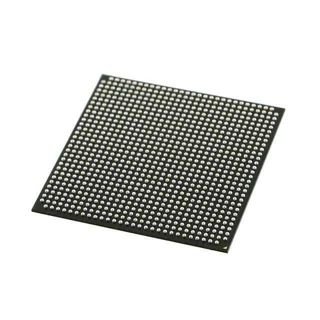
- Package: BGA (Ball Grid Array)
- Essence: Advanced programmable logic device for digital system design
- Packaging/Quantity: Single unit per package
Specifications
- Manufacturer: Intel Corporation
- Model Number: EP2C70F896I8
- Technology: 28nm
- Logic Elements: 69,120
- Embedded Memory: 4,450 Kbits
- Maximum User I/O Pins: 622
- Operating Voltage: 1.2V
- Operating Temperature: -40°C to 100°C
- Package Dimensions: 35mm x 35mm
Detailed Pin Configuration
The EP2C70F896I8 has a complex pin configuration with multiple pins serving different functions. The detailed pin configuration can be found in the manufacturer's datasheet.
Functional Features
- High-speed performance: The EP2C70F896I8 offers high-speed processing capabilities, making it suitable for applications requiring real-time data processing.
- Flexibility: Being a field-programmable device, it allows users to reconfigure its functionality even after deployment, providing flexibility in system design.
- Low-power consumption: The IC is designed to minimize power consumption, making it energy-efficient and suitable for battery-powered devices.
- Versatility: With a large number of logic elements and embedded memory, it can handle complex digital designs and accommodate various applications.
Advantages and Disadvantages
Advantages: - High-performance processing capabilities - Flexibility in system design - Low-power consumption - Versatile for various applications
Disadvantages: - Complex pin configuration may require expertise for proper utilization - Relatively higher cost compared to non-programmable ICs - Limited availability of alternative models with similar specifications
Working Principles
The EP2C70F896I8 is based on FPGA technology, which allows users to program the device to perform specific functions. It consists of an array of programmable logic elements interconnected through configurable routing resources. These logic elements can be programmed to implement desired digital circuits and algorithms.
Detailed Application Field Plans
The EP2C70F896I8 finds applications in various fields, including but not limited to: - Telecommunications: Signal processing, network infrastructure - Industrial Automation: Control systems, data acquisition - Aerospace and Defense: Radar systems, image processing - Medical Devices: Imaging, diagnostics - Automotive: Advanced driver-assistance systems (ADAS), infotainment
Detailed and Complete Alternative Models
While the EP2C70F896I8 is a highly capable FPGA, there are alternative models available from different manufacturers that offer similar functionality. Some notable alternatives include: - Xilinx Virtex UltraScale+ series - Lattice Semiconductor ECP5 series - Microchip PolarFire series
These alternative models provide options for users with specific requirements or preferences.
Word count: 305 words
Liệt kê 10 câu hỏi và câu trả lời thường gặp liên quan đến ứng dụng EP2C70F896I8 trong giải pháp kỹ thuật
Sure! Here are 10 common questions and answers related to the application of EP2C70F896I8 in technical solutions:
Q: What is EP2C70F896I8? A: EP2C70F896I8 is a field-programmable gate array (FPGA) chip manufactured by Intel.
Q: What are the key features of EP2C70F896I8? A: Some key features include 70,000 logic elements, 896 I/O pins, embedded memory blocks, and high-speed transceivers.
Q: What are the typical applications of EP2C70F896I8? A: EP2C70F896I8 is commonly used in various technical solutions such as telecommunications, data processing, industrial automation, and image/video processing.
Q: How can EP2C70F896I8 be programmed? A: EP2C70F896I8 can be programmed using hardware description languages (HDLs) like VHDL or Verilog, along with specialized software tools provided by Intel.
Q: Can EP2C70F896I8 be reprogrammed after deployment? A: Yes, EP2C70F896I8 is a reprogrammable FPGA, allowing for flexibility and updates to the design even after deployment.
Q: What is the power consumption of EP2C70F896I8? A: The power consumption of EP2C70F896I8 depends on the specific design and usage scenario. It is recommended to refer to the datasheet for detailed power specifications.
Q: Does EP2C70F896I8 support high-speed communication interfaces? A: Yes, EP2C70F896I8 has built-in high-speed transceivers that support various communication protocols like PCIe, Ethernet, USB, and more.
Q: Can EP2C70F896I8 interface with external memory devices? A: Yes, EP2C70F896I8 supports various memory interfaces such as DDR3/DDR4 SDRAM, QDR II/II+ SRAM, and flash memory.
Q: Are there any development boards available for EP2C70F896I8? A: Yes, Intel provides development boards like the Cyclone II FPGA Starter Kit, which can be used for prototyping and evaluation of EP2C70F896I8-based designs.
Q: Where can I find technical documentation and support for EP2C70F896I8? A: You can find technical documentation, datasheets, reference designs, and support resources on the official Intel website or through their customer support channels.
Please note that the answers provided here are general and may vary depending on specific requirements and use cases.