

Xem thông số kỹ thuật để biết chi tiết sản phẩm.
EP2S30F672I4N
Product Overview
Category
The EP2S30F672I4N belongs to the category of Field-Programmable Gate Arrays (FPGAs).
Use
FPGAs are integrated circuits that can be programmed after manufacturing. The EP2S30F672I4N is specifically designed for use in various electronic systems, including telecommunications, automotive, industrial automation, and consumer electronics.
Characteristics
- High-performance FPGA with advanced features
- Offers a large number of programmable logic elements
- Provides high-speed interfaces for data transfer
- Supports complex digital designs and algorithms
- Enables rapid prototyping and system development
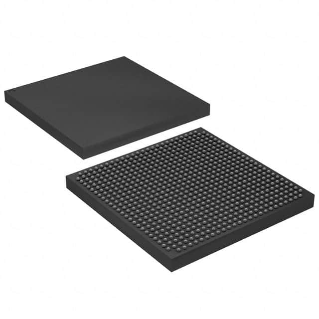
Package
The EP2S30F672I4N comes in a compact and durable package, ensuring easy integration into electronic systems. It is available in a plastic ball grid array (BGA) package.
Essence
The essence of the EP2S30F672I4N lies in its ability to provide flexible and customizable digital circuitry, allowing designers to implement complex functionalities without the need for custom hardware.
Packaging/Quantity
The EP2S30F672I4N is typically sold in reels or trays, depending on the manufacturer's packaging standards. The quantity per package may vary, but it is commonly available in quantities suitable for both small-scale and large-scale production.
Specifications
- Logic Elements: 30,000
- Embedded Memory: 1,536 Kbits
- Maximum User I/Os: 622
- Clock Management Tiles: 8
- DSP Blocks: 96
- Maximum Operating Frequency: 550 MHz
- Operating Voltage: 1.2V
- Package Type: BGA
- Package Pins: 672
Detailed Pin Configuration
The EP2S30F672I4N has a total of 672 pins, each serving a specific purpose in the FPGA's functionality. The pin configuration includes input/output pins, power supply pins, ground pins, and configuration pins. A detailed pinout diagram can be found in the product datasheet.
Functional Features
1. High-Speed Interfaces
The EP2S30F672I4N supports various high-speed interfaces, including DDR3 memory interfaces, PCIe, Ethernet, and USB. This enables seamless integration with modern communication protocols and data transfer standards.
2. Flexible Logic Elements
With 30,000 programmable logic elements, designers have the freedom to implement complex digital designs and algorithms. This flexibility allows for efficient resource utilization and customization according to specific application requirements.
3. Clock Management Tiles
The FPGA incorporates 8 clock management tiles, which provide advanced clocking features such as phase-locked loops (PLLs) and delay-locked loops (DLLs). These features ensure precise timing control and synchronization within the system.
4. DSP Blocks
The EP2S30F672I4N includes 96 dedicated digital signal processing (DSP) blocks. These blocks offer optimized arithmetic functions, making it ideal for applications requiring high-performance signal processing capabilities.
Advantages and Disadvantages
Advantages
- Versatile and flexible design options
- High-performance capabilities
- Rapid prototyping and development
- Integration of complex functionalities
- Support for various high-speed interfaces
Disadvantages
- Steeper learning curve compared to traditional ASIC or microcontroller-based designs
- Higher power consumption compared to low-power specialized devices
- Limited availability of alternative models with similar specifications
Working Principles
The EP2S30F672I4N operates based on the principles of reconfigurable computing. It consists of an array of programmable logic elements interconnected through configurable routing resources. The device is programmed using hardware description languages (HDLs) such as VHDL or Verilog, which define the desired functionality and interconnections within the FPGA.
During operation, the programmed configuration is loaded into the FPGA, enabling it to perform the desired digital functions. The flexibility of FPGAs allows for iterative design changes without the need for physical hardware modifications, making them highly adaptable for various applications.
Detailed Application Field Plans
The EP2S30F672I4N finds extensive application in several fields, including:
- Telecommunications: Used in base stations, routers, and network switches for high-speed data processing and protocol handling.
- Automotive: Employed in advanced driver-assistance systems (ADAS), infotainment systems, and engine control units (ECUs) for real-time signal processing and control.
- Industrial Automation: Utilized in programmable logic controllers (PLCs), motor control systems, and robotics for precise control and automation tasks.
- Consumer Electronics: Integrated into smart TVs, gaming consoles, and multimedia devices for high-performance video and audio processing.
Detailed and Complete Alternative Models
While the EP2S30F672I4N offers a unique combination
Liệt kê 10 câu hỏi và câu trả lời thường gặp liên quan đến ứng dụng EP2S30F672I4N trong giải pháp kỹ thuật
Sure! Here are 10 common questions and answers related to the application of EP2S30F672I4N in technical solutions:
Q: What is EP2S30F672I4N? A: EP2S30F672I4N is a field-programmable gate array (FPGA) manufactured by Intel (formerly Altera). It is a versatile integrated circuit that can be programmed to perform various digital logic functions.
Q: What are the key features of EP2S30F672I4N? A: Some key features of EP2S30F672I4N include 30,000 logic elements, 672 user I/O pins, embedded memory blocks, high-speed transceivers, and support for various communication protocols.
Q: In what applications can EP2S30F672I4N be used? A: EP2S30F672I4N can be used in a wide range of applications such as telecommunications, industrial automation, automotive electronics, medical devices, aerospace systems, and many more.
Q: How can EP2S30F672I4N be programmed? A: EP2S30F672I4N can be programmed using hardware description languages (HDLs) like VHDL or Verilog. The programming is typically done using specialized software tools provided by Intel.
Q: Can EP2S30F672I4N be reprogrammed after it has been programmed once? A: Yes, EP2S30F672I4N is a reprogrammable FPGA. It can be erased and reprogrammed multiple times, allowing for flexibility and iterative development.
Q: What kind of peripherals can be interfaced with EP2S30F672I4N? A: EP2S30F672I4N supports various standard interfaces such as UART, SPI, I2C, Ethernet, USB, and PCIe. It can also be used to interface with custom peripherals using the available I/O pins.
Q: How does EP2S30F672I4N compare to other FPGAs in terms of performance? A: EP2S30F672I4N offers a good balance between cost and performance. While it may not have the highest logic capacity or fastest speeds compared to some high-end FPGAs, it is suitable for many mid-range applications.
Q: Are there any development boards or evaluation kits available for EP2S30F672I4N? A: Yes, Intel provides development boards and evaluation kits specifically designed for EP2S30F672I4N. These kits often include necessary software tools, documentation, and example projects to get started.
Q: Can EP2S30F672I4N be used in safety-critical applications? A: Yes, EP2S30F672I4N can be used in safety-critical applications. However, additional measures like redundancy, fault tolerance, and thorough testing should be implemented to ensure reliability.
Q: Where can I find technical support or documentation for EP2S30F672I4N? A: Intel provides comprehensive technical support, documentation, datasheets, application notes, and user guides for EP2S30F672I4N on their official website. Additionally, online forums and communities can also be helpful for getting assistance from experienced users.