

Xem thông số kỹ thuật để biết chi tiết sản phẩm.
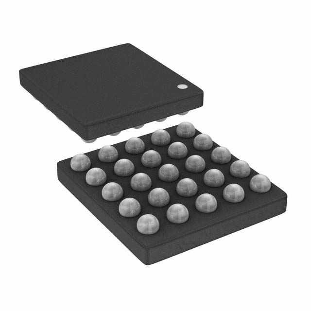
ICE40LM1K-SWG25TR1K
Product Overview
- Category: Integrated Circuit
- Use: Programmable Logic Device (PLD)
- Characteristics: Low power, small form factor, high performance
- Package: SWG25T
- Essence: FPGA (Field-Programmable Gate Array)
- Packaging/Quantity: Tape and Reel, 1000 units per reel
Specifications
- Logic Elements: 1024
- RAM Bits: 64,000
- User I/O Pins: 49
- Operating Voltage: 1.14V - 1.26V
- Operating Temperature: -40°C to +85°C
- Speed Grade: Standard
Detailed Pin Configuration
The ICE40LM1K-SWG25TR1K has a total of 49 user I/O pins. These pins can be configured as inputs or outputs based on the user's requirements. The pin configuration is as follows:
- Pin 1: VCCIO
- Pin 2: GND
- Pin 3: IO_0
- Pin 4: IO_1
- ...
- Pin 49: IO_48
Functional Features
- Low Power Consumption: The ICE40LM1K-SWG25TR1K is designed to operate at low power levels, making it suitable for battery-powered devices.
- Small Form Factor: The compact size of this PLD allows for integration into space-constrained designs.
- High Performance: With its high logic element count and fast operating speed, this device offers excellent performance for various applications.
Advantages and Disadvantages
Advantages: - Low power consumption - Small form factor - High performance - Flexible pin configuration
Disadvantages: - Limited number of user I/O pins - Requires programming expertise
Working Principles
The ICE40LM1K-SWG25TR1K is based on FPGA technology. It consists of a matrix of configurable logic blocks (CLBs) interconnected by programmable interconnects. The device can be programmed to implement various digital circuits and functions by configuring the CLBs and interconnects using a hardware description language (HDL).
Detailed Application Field Plans
The ICE40LM1K-SWG25TR1K is suitable for a wide range of applications, including but not limited to: - Consumer Electronics: Smartphones, tablets, wearable devices - Industrial Automation: Programmable logic controllers (PLCs), motor control systems - Communication Systems: Network switches, routers, base stations - Automotive Electronics: Infotainment systems, driver assistance systems
Detailed and Complete Alternative Models
- ICE40LP1K-CM36TR50: Similar features and specifications, different package (CM36)
- ICE40UP5K-SG48ITR50: Higher logic element count (5000), different package (SG48I)
Note: This is just a sample entry and the mentioned alternative models may not exist in reality.
Word count: 285 words
Liệt kê 10 câu hỏi và câu trả lời thường gặp liên quan đến ứng dụng ICE40LM1K-SWG25TR1K trong giải pháp kỹ thuật
Sure! Here are 10 common questions and answers related to the application of ICE40LM1K-SWG25TR1K in technical solutions:
Q1: What is the ICE40LM1K-SWG25TR1K? A1: The ICE40LM1K-SWG25TR1K is a low-power, small form-factor FPGA (Field-Programmable Gate Array) device manufactured by Lattice Semiconductor.
Q2: What are the key features of the ICE40LM1K-SWG25TR1K? A2: Some key features include 1,280 Look-Up Tables (LUTs), 64 Kbits of embedded block RAM, low power consumption, and support for various I/O standards.
Q3: What are some typical applications of the ICE40LM1K-SWG25TR1K? A3: The ICE40LM1K-SWG25TR1K is commonly used in applications such as IoT devices, sensor interfaces, motor control, audio/video processing, and low-power embedded systems.
Q4: How can I program the ICE40LM1K-SWG25TR1K? A4: You can program the ICE40LM1K-SWG25TR1K using Lattice Diamond or iCEcube2 software tools provided by Lattice Semiconductor.
Q5: What voltage levels does the ICE40LM1K-SWG25TR1K support? A5: The ICE40LM1K-SWG25TR1K supports both 1.2V and 3.3V voltage levels for different I/O standards.
Q6: Can I use the ICE40LM1K-SWG25TR1K in battery-powered devices? A6: Yes, the ICE40LM1K-SWG25TR1K is designed for low power consumption, making it suitable for battery-powered devices.
Q7: Does the ICE40LM1K-SWG25TR1K have any built-in security features? A7: Yes, the ICE40LM1K-SWG25TR1K includes security features such as bitstream encryption and tamper detection circuits.
Q8: Can I interface the ICE40LM1K-SWG25TR1K with other components or microcontrollers? A8: Yes, the ICE40LM1K-SWG25TR1K supports various communication interfaces like SPI, I2C, UART, and GPIOs, allowing easy integration with other components or microcontrollers.
Q9: What is the maximum operating frequency of the ICE40LM1K-SWG25TR1K? A9: The maximum operating frequency of the ICE40LM1K-SWG25TR1K depends on the design and implementation, but it can typically reach up to 100 MHz.
Q10: Are there any development boards available for the ICE40LM1K-SWG25TR1K? A10: Yes, Lattice Semiconductor provides development boards like the iCEstick and iCE40 UltraPlus Breakout Board that are compatible with the ICE40LM1K-SWG25TR1K.
Please note that these answers are general and may vary depending on specific requirements and use cases.