

Xem thông số kỹ thuật để biết chi tiết sản phẩm.
ICE40LM2K-CM49
Product Overview
Category
The ICE40LM2K-CM49 belongs to the category of programmable logic devices (PLDs).
Use
This device is primarily used for implementing digital logic circuits in various electronic applications.
Characteristics
- Programmable: The ICE40LM2K-CM49 can be configured to perform specific functions based on user requirements.
- Low power consumption: This device is designed to operate efficiently with minimal power consumption.
- High performance: It offers fast processing speeds and reliable operation.
- Compact package: The ICE40LM2K-CM49 is available in a small form factor, making it suitable for space-constrained designs.
- Versatile: It supports a wide range of applications due to its flexible programming capabilities.
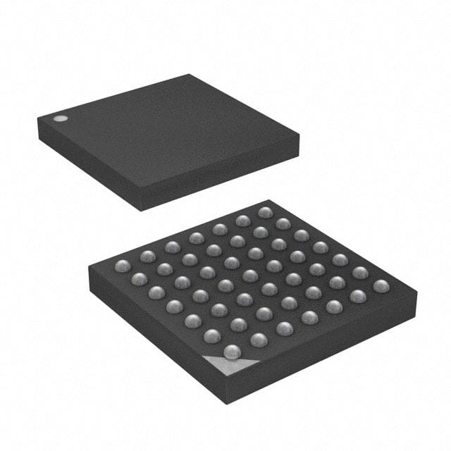
Package
The ICE40LM2K-CM49 is packaged in a CM49 package type.
Essence
The essence of the ICE40LM2K-CM49 lies in its ability to provide a customizable and efficient solution for digital circuit implementation.
Packaging/Quantity
This device is typically sold in reels or trays, with a quantity of 1000 units per reel/tray.
Specifications
- Logic elements: 2000
- User I/Os: 49
- Block RAM: 64 Kbits
- Clock management: PLLs, DLLs
- Operating voltage: 1.2V
- Operating temperature range: -40°C to 85°C
- Package dimensions: 7mm x 7mm
Detailed Pin Configuration
The ICE40LM2K-CM49 features the following pin configuration:
| Pin Name | Description | |----------|-------------| | VCC | Power supply input | | GND | Ground reference | | IO[0:48] | User I/O pins | | CLK | Clock input | | RESET | Reset input | | ... | Additional pins |
Functional Features
- Programmable logic: The ICE40LM2K-CM49 offers a large number of logic elements for implementing complex digital circuits.
- Clock management: It includes PLLs and DLLs for precise clock generation and distribution.
- Block RAM: This device provides 64 Kbits of on-chip memory for data storage.
- I/O capabilities: With 49 user I/O pins, it allows for versatile interfacing with external devices.
- Low power consumption: The ICE40LM2K-CM49 is designed to operate efficiently, minimizing power consumption.
Advantages and Disadvantages
Advantages
- Versatile programmability enables customization for various applications.
- Compact package size facilitates integration into space-constrained designs.
- Low power consumption extends battery life in portable devices.
- High-performance logic elements ensure fast and reliable operation.
Disadvantages
- Limited number of user I/O pins may restrict connectivity options in complex designs.
- Lack of built-in peripherals may require additional components for certain applications.
Working Principles
The ICE40LM2K-CM49 utilizes a field-programmable gate array (FPGA) architecture. It consists of configurable logic blocks interconnected through programmable routing resources. The device can be programmed using hardware description languages (HDL) or schematic entry tools. Once programmed, the FPGA configuration remains persistent until reprogrammed.
Detailed Application Field Plans
The ICE40LM2K-CM49 finds applications in various fields, including:
- Communications: Used in networking equipment, routers, and switches for data processing and protocol handling.
- Consumer electronics: Integrated into smart home devices, wearable gadgets, and multimedia systems for control and signal processing.
- Industrial automation: Employed in programmable logic controllers (PLCs), motor control systems, and industrial monitoring equipment.
- Automotive: Utilized in automotive electronics for engine control, driver assistance systems, and infotainment systems.
- Medical devices: Integrated into medical imaging equipment, patient monitoring systems, and laboratory instruments.
Detailed and Complete Alternative Models
- ICE40LP2K-CM36: Similar to the ICE40LM2K-CM49 but with 2000 logic elements and 36 user I/Os.
- ICE40UP5K-SG48: Offers 5280 logic elements and 45 user I/Os, suitable for more complex designs.
- ICE40HX8K-CM225: Provides 7680 logic elements and 225 user I/Os, ideal for large-scale applications.
These alternative models offer varying capabilities and pin configurations to cater to different project requirements.
In conclusion, the ICE40LM2K-CM49 is a versatile programmable logic device that offers high performance and low power consumption. Its compact package and flexible programming capabilities make it suitable for a wide range of applications in various industries.
Liệt kê 10 câu hỏi và câu trả lời thường gặp liên quan đến ứng dụng ICE40LM2K-CM49 trong giải pháp kỹ thuật
Sure! Here are 10 common questions and answers related to the application of ICE40LM2K-CM49 in technical solutions:
Q: What is ICE40LM2K-CM49? A: ICE40LM2K-CM49 is a low-power FPGA (Field-Programmable Gate Array) device manufactured by Lattice Semiconductor.
Q: What are the key features of ICE40LM2K-CM49? A: Some key features of ICE40LM2K-CM49 include 3840 Look-Up Tables (LUTs), 49 I/O pins, low power consumption, and small form factor.
Q: What are the typical applications of ICE40LM2K-CM49? A: ICE40LM2K-CM49 is commonly used in applications such as IoT devices, sensor interfaces, motor control, portable medical devices, and more.
Q: How can I program ICE40LM2K-CM49? A: ICE40LM2K-CM49 can be programmed using Lattice Diamond or iCEcube2 software tools provided by Lattice Semiconductor.
Q: What is the power consumption of ICE40LM2K-CM49? A: The power consumption of ICE40LM2K-CM49 depends on the design and operating conditions, but it is generally known for its low power characteristics.
Q: Can I use ICE40LM2K-CM49 in battery-powered devices? A: Yes, ICE40LM2K-CM49 is suitable for battery-powered devices due to its low power consumption, making it an ideal choice for energy-efficient designs.
Q: Does ICE40LM2K-CM49 support external memory interfaces? A: Yes, ICE40LM2K-CM49 supports various external memory interfaces such as SPI, I2C, and UART, allowing for easy integration with other devices.
Q: What is the maximum operating frequency of ICE40LM2K-CM49? A: The maximum operating frequency of ICE40LM2K-CM49 depends on the design and implementation, but it can typically reach frequencies up to 100 MHz or higher.
Q: Can I use ICE40LM2K-CM49 for real-time signal processing applications? A: Yes, ICE40LM2K-CM49 can be used for real-time signal processing applications due to its high-speed capabilities and flexible programmability.
Q: Are there any development boards available for ICE40LM2K-CM49? A: Yes, Lattice Semiconductor provides development boards like iCE40 UltraPlus Breakout Board that support ICE40LM2K-CM49, making it easier for prototyping and evaluation.
Please note that these answers are general and may vary depending on specific requirements and use cases.