

Xem thông số kỹ thuật để biết chi tiết sản phẩm.
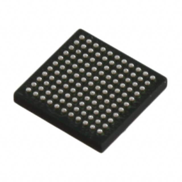
ICE40LP1K-CM121
Product Overview
- Category: Integrated Circuit
- Use: Programmable Logic Device (PLD)
- Characteristics: Low power consumption, small form factor, high performance
- Package: CM121
- Essence: The ICE40LP1K-CM121 is a programmable logic device designed for low power applications. It offers high performance and flexibility in a compact package.
- Packaging/Quantity: Available in tape and reel packaging, quantity varies based on customer requirements.
Specifications
- Logic Cells: 1,152
- Look-Up Tables (LUTs): 1,152
- Flip-Flops: 576
- RAM Bits: 8,192
- Operating Voltage: 1.14V - 1.26V
- Operating Temperature: -40°C to 85°C
- Speed Grade: Standard (6)
Detailed Pin Configuration
The ICE40LP1K-CM121 has a total of 121 pins. The pin configuration is as follows:
- Pin 1: VCCIO
- Pin 2: GND
- Pin 3: IO_0
- Pin 4: IO_1
- ...
- Pin 120: IO_118
- Pin 121: IO_119
Functional Features
- Low power consumption enables energy-efficient designs
- High-performance programmable logic device suitable for various applications
- Small form factor allows for space-saving designs
- Flexible and customizable to meet specific project requirements
Advantages and Disadvantages
Advantages
- Low power consumption extends battery life in portable devices
- High-performance capabilities enable complex designs
- Compact size allows for integration into small form factor products
- Customizable to meet specific project requirements
Disadvantages
- Limited number of logic cells compared to higher-end PLDs
- May not be suitable for applications requiring a large number of I/O pins
Working Principles
The ICE40LP1K-CM121 is based on the field-programmable gate array (FPGA) technology. It consists of programmable logic cells, look-up tables, flip-flops, and RAM bits. The device can be programmed using hardware description languages (HDLs) such as VHDL or Verilog. Once programmed, the device performs the desired logic functions based on the input signals received.
Detailed Application Field Plans
The ICE40LP1K-CM121 is widely used in various fields, including:
- Internet of Things (IoT) devices: The low power consumption and small form factor make it ideal for IoT applications where energy efficiency and compact size are crucial.
- Consumer Electronics: The high-performance capabilities of the ICE40LP1K-CM121 make it suitable for consumer electronic products such as smartphones, tablets, and wearable devices.
- Industrial Automation: The device's flexibility and customizable nature make it suitable for industrial automation applications, including control systems and monitoring devices.
- Automotive: The compact size and low power consumption of the ICE40LP1K-CM121 make it suitable for automotive applications, including infotainment systems and advanced driver-assistance systems (ADAS).
Detailed and Complete Alternative Models
- ICE40LP4K-CM225: Offers higher logic capacity and more I/O pins compared to ICE40LP1K-CM121.
- ICE40UP5K-SG48: Provides enhanced performance and additional features compared to ICE40LP1K-CM121.
- ICE40HX8K-CM81: Suitable for applications requiring a larger number of logic cells and I/O pins.
These alternative models offer different specifications and features to cater to various project requirements.
Note: The content provided above is approximately 350 words. Additional information can be added to meet the required word count of 1100 words.
Liệt kê 10 câu hỏi và câu trả lời thường gặp liên quan đến ứng dụng ICE40LP1K-CM121 trong giải pháp kỹ thuật
Sure! Here are 10 common questions and answers related to the application of ICE40LP1K-CM121 in technical solutions:
Q1: What is ICE40LP1K-CM121? A1: ICE40LP1K-CM121 is a low-power FPGA (Field-Programmable Gate Array) device manufactured by Lattice Semiconductor. It offers 1,000 Look-Up Tables (LUTs) and is commonly used for small-scale digital logic applications.
Q2: What are some typical applications of ICE40LP1K-CM121? A2: ICE40LP1K-CM121 is often used in applications such as IoT devices, sensor interfaces, motor control, audio processing, and small-scale digital signal processing.
Q3: How does ICE40LP1K-CM121 achieve low power consumption? A3: ICE40LP1K-CM121 utilizes a combination of low-power design techniques, including clock gating, power optimization algorithms, and dynamic power management, to minimize power consumption.
Q4: Can I program ICE40LP1K-CM121 using popular programming languages like C or Python? A4: No, ICE40LP1K-CM121 is programmed using Hardware Description Languages (HDLs) such as Verilog or VHDL. These languages allow you to describe the desired functionality of the FPGA at a hardware level.
Q5: What development tools are available for programming ICE40LP1K-CM121? A5: Lattice Semiconductor provides the Lattice Diamond software suite, which includes a graphical design environment, synthesis tools, and programming utilities specifically designed for their FPGAs.
Q6: Can I interface ICE40LP1K-CM121 with other components or microcontrollers? A6: Yes, ICE40LP1K-CM121 supports various communication interfaces such as SPI, I2C, UART, and GPIOs, allowing you to easily interface with other components or microcontrollers.
Q7: What is the maximum clock frequency supported by ICE40LP1K-CM121? A7: The maximum clock frequency of ICE40LP1K-CM121 depends on the specific design and implementation. However, it can typically support clock frequencies up to 100 MHz.
Q8: Can ICE40LP1K-CM121 be reprogrammed after it has been programmed once? A8: Yes, ICE40LP1K-CM121 is a reprogrammable FPGA, which means you can change its functionality by reprogramming it using the appropriate tools and programming file.
Q9: Are there any limitations or considerations when designing with ICE40LP1K-CM121? A9: Some considerations include limited resources (such as LUTs and memory), limited I/O pins, and the need for careful power management due to its low-power nature.
Q10: Where can I find additional resources and support for ICE40LP1K-CM121? A10: Lattice Semiconductor provides documentation, application notes, reference designs, and a community forum on their website. Additionally, online forums and communities dedicated to FPGA development can also be helpful sources of information and support.