

Xem thông số kỹ thuật để biết chi tiết sản phẩm.
LC4064B-25T44C
Product Overview
Category: Integrated Circuit (IC)
Use: The LC4064B-25T44C is a programmable logic device (PLD) that belongs to the family of Complex Programmable Logic Devices (CPLDs). It is designed for digital logic applications and offers high-performance, low-power consumption, and flexibility in circuit design.
Characteristics: - High-density integration - Low power consumption - Fast propagation delay - Flexible programming options - Wide operating temperature range
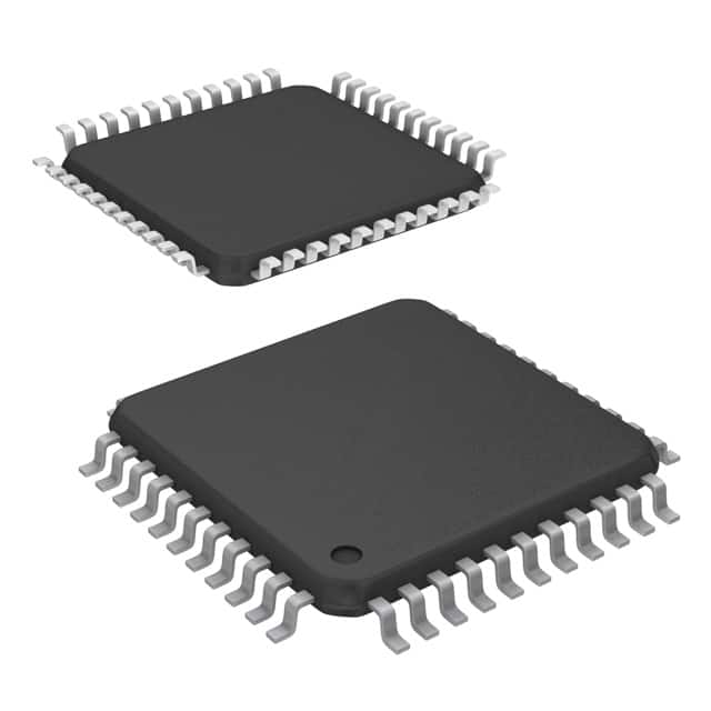
Package: The LC4064B-25T44C is available in a 44-pin Thin Quad Flat Pack (TQFP) package. This package provides ease of handling and compatibility with standard surface mount technology.
Essence: The essence of the LC4064B-25T44C lies in its ability to implement complex digital logic functions in a single integrated circuit. It offers designers the flexibility to create custom logic circuits tailored to their specific application requirements.
Packaging/Quantity: The LC4064B-25T44C is typically supplied in reels or tubes, with a quantity of 250 units per reel/tube.
Specifications
- Operating Voltage: 3.3V
- Maximum Operating Frequency: 25 MHz
- Number of Logic Cells: 64
- Number of I/O Pins: 36
- Programmable Macrocells: 32
- On-Chip Memory: 1,024 bits
- JTAG Boundary Scan Support: Yes
- Package Dimensions: 10mm x 10mm
Pin Configuration
The LC4064B-25T44C has a total of 44 pins. The pin configuration is as follows:
Pin 1: VCCIO
Pin 2: GND
Pin 3: IO0
Pin 4: IO1
...
Pin 43: IO34
Pin 44: IO35
For a detailed pinout diagram, please refer to the LC4064B-25T44C datasheet.
Functional Features
The LC4064B-25T44C offers several functional features that enhance its usability and performance:
- Programmability: The device can be programmed using industry-standard hardware description languages (HDLs) such as VHDL or Verilog, allowing designers to create custom logic functions.
- Flexible I/O Configuration: The device supports a wide range of I/O standards, including LVTTL, LVCMOS, and SSTL, providing compatibility with various external devices.
- Clock Management: The LC4064B-25T44C includes dedicated clock management resources, such as PLLs (Phase-Locked Loops), enabling precise timing control in complex designs.
- Embedded Memory: With on-chip memory, the device can store configuration data, lookup tables, or other user-defined data, reducing the need for external memory components.
- JTAG Boundary Scan: The built-in JTAG boundary scan support allows for easy testing and debugging of the device during development and production stages.
Advantages and Disadvantages
Advantages: - High integration density enables complex circuit implementation in a single device. - Low power consumption makes it suitable for battery-powered applications. - Flexible programming options provide design flexibility and adaptability. - Fast propagation delay ensures high-speed operation. - Wide operating temperature range allows for use in various environments.
Disadvantages: - Limited number of logic cells may restrict the complexity of certain designs. - Programming and debugging processes may require specialized knowledge and tools. - Higher cost compared to simpler programmable logic devices.
Working Principles
The LC4064B-25T44C operates based on the principles of programmable logic. It consists of an array of configurable logic blocks (CLBs) interconnected through a programmable routing matrix. The CLBs contain look-up tables (LUTs), flip-flops, and other resources that can be configured to implement desired logic functions.
During programming, the device is loaded with a configuration bitstream that defines the desired logic circuit. This bitstream configures the interconnections between CLBs and sets the functionality of each CLB's LUTs and flip-flops. Once programmed, the LC4064B-25T44C operates as a dedicated digital logic circuit, executing the desired functions.
Detailed Application Field Plans
The LC4064B-25T44C finds applications in various fields, including:
- Embedded Systems: It can be used in embedded systems for control and interfacing purposes, providing custom logic functions tailored to specific requirements.
- Communications: The device can be employed in communication systems for protocol handling, data processing, and signal conditioning tasks.
- Industrial Automation: It enables the implementation of complex control algorithms and logic circuits in industrial automation systems
Liệt kê 10 câu hỏi và câu trả lời thường gặp liên quan đến ứng dụng LC4064B-25T44C trong giải pháp kỹ thuật
Sure! Here are 10 common questions and answers related to the application of LC4064B-25T44C in technical solutions:
Q: What is LC4064B-25T44C? A: LC4064B-25T44C is a specific model of a field-programmable gate array (FPGA) manufactured by Lattice Semiconductor.
Q: What are the key features of LC4064B-25T44C? A: LC4064B-25T44C features 64 macrocells, 64 input/output pins, a maximum operating frequency of 25 MHz, and a TQFP-44 package.
Q: What are the typical applications of LC4064B-25T44C? A: LC4064B-25T44C is commonly used in various technical solutions such as industrial control systems, communication equipment, automotive electronics, and consumer electronics.
Q: How can LC4064B-25T44C be programmed? A: LC4064B-25T44C can be programmed using hardware description languages (HDLs) like VHDL or Verilog, or through graphical programming tools provided by Lattice Semiconductor.
Q: What is the power supply requirement for LC4064B-25T44C? A: LC4064B-25T44C requires a power supply voltage of 3.3V.
Q: Can LC4064B-25T44C be reprogrammed after initial programming? A: Yes, LC4064B-25T44C is a reprogrammable FPGA, allowing for multiple programming cycles.
Q: Are there any development boards available for LC4064B-25T44C? A: Yes, Lattice Semiconductor provides development boards specifically designed for LC4064B-25T44C, which can aid in prototyping and testing.
Q: What are the advantages of using LC4064B-25T44C in technical solutions? A: LC4064B-25T44C offers flexibility, high performance, and low power consumption, making it suitable for a wide range of applications. It also allows for rapid prototyping and reduces time-to-market.
Q: Can LC4064B-25T44C interface with other components or devices? A: Yes, LC4064B-25T44C supports various communication protocols such as SPI, I2C, UART, and GPIO, enabling seamless integration with other components or devices.
Q: Where can I find documentation and support for LC4064B-25T44C? A: Documentation, datasheets, application notes, and technical support for LC4064B-25T44C can be found on the official website of Lattice Semiconductor or by contacting their customer support team.