

Xem thông số kỹ thuật để biết chi tiết sản phẩm.
LCMXO2-1200ZE-1UWG25ITR1K
Product Overview
Category: Programmable Logic Device (PLD)
Use: The LCMXO2-1200ZE-1UWG25ITR1K is a PLD that can be programmed to perform various logic functions. It is commonly used in digital circuit design and prototyping.
Characteristics: - Low power consumption - Small form factor - High performance - Flexible and reprogrammable
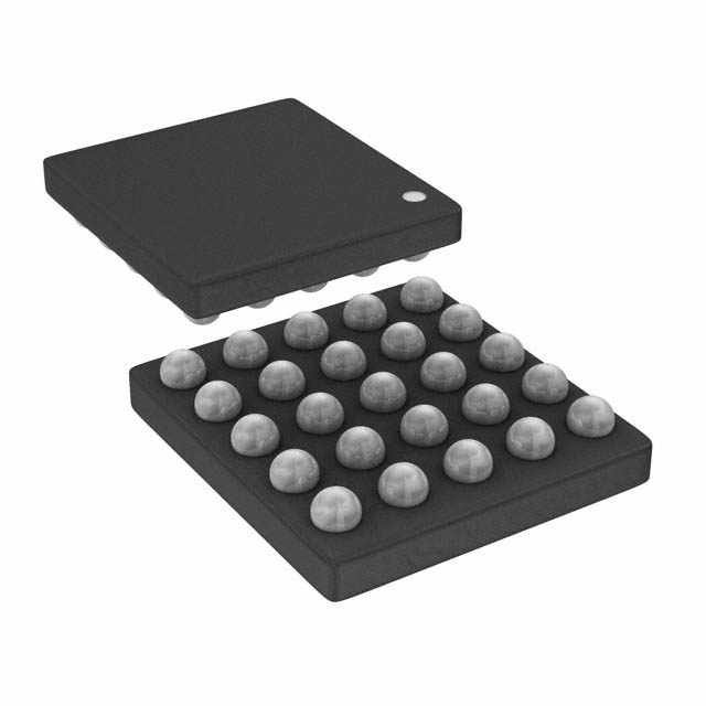
Package: The LCMXO2-1200ZE-1UWG25ITR1K comes in a small form factor package, making it suitable for applications with limited space.
Essence: The essence of the LCMXO2-1200ZE-1UWG25ITR1K lies in its ability to provide a customizable logic solution for digital circuit designers.
Packaging/Quantity: The LCMXO2-1200ZE-1UWG25ITR1K is typically sold individually or in small quantities, depending on the supplier.
Specifications
- Logic Cells: 1200
- Operating Voltage: 1.2V
- I/O Pins: 25
- Speed Grade: -1
- Package Type: UWG25
- Temperature Range: Industrial (-40°C to +85°C)
- RoHS Compliant: Yes
Detailed Pin Configuration
The LCMXO2-1200ZE-1UWG25ITR1K has a total of 25 I/O pins. The pin configuration is as follows:
- Pin 1: VCCIO
- Pin 2: GND
- Pin 3: IO_0
- Pin 4: IO_1
- Pin 5: IO_2
- Pin 6: IO_3
- Pin 7: IO_4
- Pin 8: IO_5
- Pin 9: IO_6
- Pin 10: IO_7
- Pin 11: IO_8
- Pin 12: IO_9
- Pin 13: IO_10
- Pin 14: IO_11
- Pin 15: IO_12
- Pin 16: IO_13
- Pin 17: IO_14
- Pin 18: IO_15
- Pin 19: IO_16
- Pin 20: IO_17
- Pin 21: IO_18
- Pin 22: IO_19
- Pin 23: IO_20
- Pin 24: IO_21
- Pin 25: IO_22
Functional Features
- High-speed performance
- Low power consumption
- Flexible I/O configuration
- Reprogrammable logic cells
- On-chip oscillator for clock generation
Advantages and Disadvantages
Advantages: - Small form factor allows for space-efficient designs - Low power consumption makes it suitable for battery-powered applications - Reprogrammability enables iterative design and prototyping - High-speed performance meets the requirements of demanding applications
Disadvantages: - Limited number of I/O pins may restrict the complexity of designs - Programming and debugging process can be complex for beginners - Higher cost compared to traditional fixed-function logic devices
Working Principles
The LCMXO2-1200ZE-1UWG25ITR1K is based on a field-programmable gate array (FPGA) architecture. It consists of programmable logic cells that can be interconnected to implement various logic functions. The device is programmed using a hardware description language (HDL) and the configuration is stored in non-volatile memory.
During operation, the input signals are processed through the programmable logic cells, which perform the desired logic operations. The output signals are then routed to the appropriate I/O pins for further processing or external interfacing.
Detailed Application Field Plans
The LCMXO2-1200ZE-1UWG25ITR1K finds applications in various fields, including:
- Digital circuit design and prototyping
- Embedded systems development
- Communication systems
- Industrial automation
- Robotics
- Internet of Things (IoT) devices
- Automotive electronics
Detailed and Complete Alternative Models
- LCMXO2-640HC-4SG32C: A lower-capacity PLD with 640 logic cells and 32 I/O pins.
- LCMXO2-1200HC-4TG100C: A higher-capacity PLD with 1200 logic cells and 100 I/O pins.
Liệt kê 10 câu hỏi và câu trả lời thường gặp liên quan đến ứng dụng LCMXO2-1200ZE-1UWG25ITR1K trong giải pháp kỹ thuật
Sure! Here are 10 common questions and answers related to the application of LCMXO2-1200ZE-1UWG25ITR1K in technical solutions:
Q1: What is the LCMXO2-1200ZE-1UWG25ITR1K? A1: The LCMXO2-1200ZE-1UWG25ITR1K is a low-cost, low-power FPGA (Field-Programmable Gate Array) device manufactured by Lattice Semiconductor.
Q2: What are the key features of LCMXO2-1200ZE-1UWG25ITR1K? A2: Some key features include 1200 Look-Up Tables (LUTs), 64 Kbits of embedded block RAM, 49 user I/O pins, and support for various I/O standards.
Q3: What are some typical applications of LCMXO2-1200ZE-1UWG25ITR1K? A3: This FPGA can be used in a wide range of applications such as industrial automation, consumer electronics, communication systems, and IoT devices.
Q4: How can I program the LCMXO2-1200ZE-1UWG25ITR1K? A4: You can program this FPGA using Lattice Diamond or Lattice Radiant software tools provided by Lattice Semiconductor.
Q5: What voltage levels does LCMXO2-1200ZE-1UWG25ITR1K support? A5: It supports both 3.3V and 1.2V voltage levels for different I/O banks.
Q6: Can I use LCMXO2-1200ZE-1UWG25ITR1K in battery-powered applications? A6: Yes, this FPGA is designed to be low-power and can be used in battery-powered applications.
Q7: Does LCMXO2-1200ZE-1UWG25ITR1K support any communication protocols? A7: Yes, it supports various communication protocols such as SPI, I2C, UART, and GPIO.
Q8: Can I use LCMXO2-1200ZE-1UWG25ITR1K for real-time signal processing? A8: Yes, this FPGA can be used for real-time signal processing tasks due to its high-speed performance and programmability.
Q9: What are the temperature range specifications for LCMXO2-1200ZE-1UWG25ITR1K? A9: It has an operating temperature range of -40°C to 125°C.
Q10: Are there any development boards available for LCMXO2-1200ZE-1UWG25ITR1K? A10: Yes, Lattice Semiconductor provides development boards like the iCEstick and MachXO3LF Starter Kit that can be used with this FPGA.
Please note that these answers are general and may vary depending on specific requirements and use cases.