

Xem thông số kỹ thuật để biết chi tiết sản phẩm.
LCMXO2-256HC-4MG132I
Product Overview
Category
The LCMXO2-256HC-4MG132I belongs to the category of Field-Programmable Gate Arrays (FPGAs).
Use
This FPGA is commonly used in electronic design and prototyping applications, where it provides a flexible and customizable digital logic solution.
Characteristics
- High capacity: The LCMXO2-256HC-4MG132I offers a large number of configurable logic elements, allowing for complex designs.
- Low power consumption: This FPGA is designed to operate efficiently with minimal power requirements.
- Small package size: The compact form factor of the LCMXO2-256HC-4MG132I makes it suitable for space-constrained applications.
- High-speed performance: With its advanced architecture, this FPGA can handle high-frequency operations.
Package and Quantity
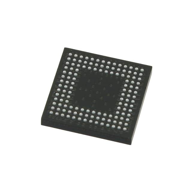
The LCMXO2-256HC-4MG132I is available in a 132-pin Quad Flat No-Lead (QFN) package. It is typically sold individually or in small quantities.
Specifications
- Logic Elements: 2560
- Look-Up Tables (LUTs): 2560
- Flip-Flops: 5120
- Block RAM: 64 Kbits
- Maximum Operating Frequency: 150 MHz
- I/O Pins: 108
- Voltage Range: 1.14V - 1.26V
- Operating Temperature Range: -40°C to 85°C
Detailed Pin Configuration
The LCMXO2-256HC-4MG132I has a total of 132 pins, each serving a specific purpose. The pin configuration includes input/output pins, power supply pins, ground pins, and configuration pins. A detailed pinout diagram can be found in the product datasheet.
Functional Features
- Programmability: The LCMXO2-256HC-4MG132I can be programmed to implement various digital logic functions, making it highly versatile.
- Reconfigurability: This FPGA allows for on-the-fly reconfiguration, enabling dynamic changes to the implemented logic.
- Embedded Memory: The built-in block RAM provides dedicated memory resources for data storage and retrieval.
- I/O Flexibility: With a wide range of I/O pins, the LCMXO2-256HC-4MG132I supports interfacing with external devices and peripherals.
Advantages and Disadvantages
Advantages
- Flexibility: The LCMXO2-256HC-4MG132I offers a high degree of flexibility in designing custom logic circuits.
- Cost-effective: FPGAs eliminate the need for custom ASICs, reducing development costs.
- Rapid Prototyping: With its reprogrammable nature, this FPGA enables quick iterations during the prototyping phase.
Disadvantages
- Complexity: Designing complex logic circuits using FPGAs requires expertise in digital design and programming.
- Limited Performance: While FPGAs offer high-speed performance, they may not match the performance of specialized ASICs for certain applications.
Working Principles
The LCMXO2-256HC-4MG132I operates based on the principles of configurable logic. It consists of an array of programmable logic elements interconnected through configurable routing resources. These logic elements can be programmed to perform specific functions, allowing for the implementation of complex digital systems.
Detailed Application Field Plans
The LCMXO2-256HC-4MG132I finds applications in various fields, including:
- Embedded Systems: This FPGA is used in embedded systems to provide customizable hardware acceleration for tasks such as image processing, signal analysis, and control systems.
- Communications: It is employed in communication systems for protocol handling, data encryption/decryption, and signal modulation/demodulation.
- Industrial Automation: The LCMXO2-256HC-4MG132I enables the implementation of custom control logic in industrial automation systems, improving efficiency and flexibility.
- Test and Measurement: This FPGA is utilized in test and measurement equipment to implement complex signal generation, data acquisition, and analysis functions.
Detailed and Complete Alternative Models
- Xilinx Spartan-6 XC6SLX9: A comparable FPGA with similar capacity and features.
- Intel Cyclone IV EP4CE6: An alternative FPGA offering a different architecture but similar capabilities.
- Microsemi IGLOO2 M2GL090: Another option with higher capacity and additional features.
These alternative models provide similar functionality to the LCMXO2-256HC-4MG132I and can be considered based on specific project requirements.
In conclusion, the LCMXO2-256HC-4MG132I is a versatile FPGA that offers high capacity, low power consumption, and flexibility in digital design applications. Its
Liệt kê 10 câu hỏi và câu trả lời thường gặp liên quan đến ứng dụng LCMXO2-256HC-4MG132I trong giải pháp kỹ thuật
Sure! Here are 10 common questions and answers related to the application of LCMXO2-256HC-4MG132I in technical solutions:
Q: What is the LCMXO2-256HC-4MG132I? A: The LCMXO2-256HC-4MG132I is a low-cost, low-power FPGA (Field-Programmable Gate Array) device manufactured by Lattice Semiconductor.
Q: What are the key features of LCMXO2-256HC-4MG132I? A: Some key features include 256 LUTs (Look-Up Tables), 2,560 logic cells, 8 multipliers, 128 Kbits of embedded memory, and support for various I/O standards.
Q: What are some typical applications of LCMXO2-256HC-4MG132I? A: It is commonly used in applications such as industrial automation, consumer electronics, communication systems, medical devices, and IoT (Internet of Things) solutions.
Q: How can I program the LCMXO2-256HC-4MG132I? A: You can program the device using Lattice Diamond or Lattice Radiant software tools, which provide a graphical interface for designing and programming the FPGA.
Q: What are the power requirements for LCMXO2-256HC-4MG132I? A: The device operates at a voltage range of 1.14V to 3.465V, with typical power consumption ranging from 25mW to 100mW, depending on the configuration.
Q: Can I use LCMXO2-256HC-4MG132I for high-speed applications? A: While it is not specifically designed for high-speed applications, it can still handle moderate-speed designs with proper optimization and careful consideration of timing constraints.
Q: Does LCMXO2-256HC-4MG132I support external memory interfaces? A: Yes, the device supports various memory interfaces such as SPI (Serial Peripheral Interface) and I2C (Inter-Integrated Circuit), allowing you to connect external memory devices.
Q: Can I use LCMXO2-256HC-4MG132I for real-time signal processing? A: Yes, the device's embedded multipliers and dedicated DSP (Digital Signal Processing) blocks make it suitable for real-time signal processing applications.
Q: What are the available package options for LCMXO2-256HC-4MG132I? A: The device is available in a 132-pin QFP (Quad Flat Package) or TQFP (Thin Quad Flat Package), which provides ease of integration into your PCB design.
Q: Are there any development boards or evaluation kits available for LCMXO2-256HC-4MG132I? A: Yes, Lattice Semiconductor offers development boards and evaluation kits that include the LCMXO2-256HC-4MG132I FPGA, allowing you to quickly prototype and test your designs.
Please note that these answers are general and may vary depending on specific requirements and application scenarios.