

Xem thông số kỹ thuật để biết chi tiết sản phẩm.
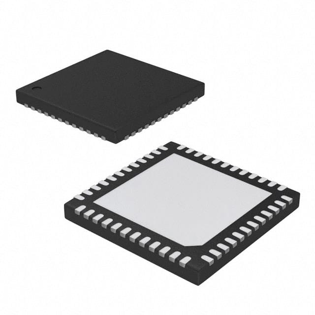
LCMXO2-256HC-4SG48I
Product Overview
Category
The LCMXO2-256HC-4SG48I belongs to the category of Field-Programmable Gate Arrays (FPGAs).
Use
This FPGA is commonly used in various electronic applications that require programmable logic devices. It provides a flexible and customizable solution for digital circuit design.
Characteristics
- High capacity: The LCMXO2-256HC-4SG48I offers a large number of logic elements, allowing for complex designs.
- Low power consumption: This FPGA is designed to operate efficiently with minimal power requirements.
- Small form factor: The compact package size makes it suitable for space-constrained applications.
- High-speed performance: The LCMXO2-256HC-4SG48I can handle high-frequency signals, enabling rapid data processing.
Package and Quantity
The LCMXO2-256HC-4SG48I is available in a 48-pin small-grid array (SGA) package. Each package contains one unit of the FPGA.
Specifications
- Logic Elements: 256
- I/O Pins: 48
- Operating Voltage: 1.2V
- Maximum Frequency: 100 MHz
- Configuration Memory: Flash-based
Pin Configuration
The pin configuration of the LCMXO2-256HC-4SG48I FPGA is as follows:
| Pin Number | Pin Name | Function | |------------|----------|----------| | 1 | VCC | Power Supply (1.2V) | | 2 | GND | Ground | | 3 | IO0 | Input/Output Pin 0 | | 4 | IO1 | Input/Output Pin 1 | | ... | ... | ... | | 48 | IO47 | Input/Output Pin 47 |
Functional Features
- Programmable Logic: The LCMXO2-256HC-4SG48I allows users to implement custom logic functions using its programmable fabric.
- I/O Flexibility: It provides a wide range of input/output pins, enabling connectivity with external devices and circuits.
- Embedded Memory: This FPGA includes embedded memory blocks for storing data or configuration information.
- Clock Management: It offers built-in clock management resources, allowing precise control over timing requirements.
Advantages and Disadvantages
Advantages
- Versatility: The LCMXO2-256HC-4SG48I can be reprogrammed multiple times, making it suitable for prototyping and iterative design processes.
- Cost-effective: FPGAs offer a cost-effective alternative to application-specific integrated circuits (ASICs) for small to medium-scale production runs.
- Rapid Development: The programmable nature of FPGAs enables faster development cycles compared to traditional hardware design methods.
Disadvantages
- Limited Performance: FPGAs may not match the performance levels of dedicated ASICs for highly specialized applications.
- Design Complexity: Utilizing FPGAs requires expertise in digital circuit design and programming languages specific to FPGA development.
Working Principles
The LCMXO2-256HC-4SG48I operates based on the principles of configurable logic. It consists of an array of programmable logic elements interconnected through configurable routing resources. These logic elements can be programmed to perform various functions, such as arithmetic operations, data storage, and signal processing. The configuration of the FPGA is stored in non-volatile memory and can be modified as needed.
Application Field Plans
The LCMXO2-256HC-4SG48I finds applications in various fields, including:
- Embedded Systems: It can be used to implement custom logic in embedded systems, such as industrial control systems and IoT devices.
- Communications: The FPGA's high-speed performance makes it suitable for applications in telecommunications and networking equipment.
- Signal Processing: It can be utilized for real-time signal processing tasks, including audio/video processing and image recognition.
- Prototyping: The LCMXO2-256HC-4SG48I is commonly used in prototyping electronic circuits due to its reprogrammable nature.
Alternative Models
Other alternative models with similar capabilities to the LCMXO2-256HC-4SG48I include:
- Xilinx Spartan-6 XC6SLX9
- Altera Cyclone IV EP4CE6
- Microsemi IGLOO2 M2GL090
These alternatives offer comparable features and can be considered based on specific project requirements.
In conclusion, the LCMXO2-256HC-4SG48I FPGA provides a versatile and cost-effective solution for digital circuit design. Its high capacity, low power consumption, and small form factor make it suitable for various applications. However
Liệt kê 10 câu hỏi và câu trả lời thường gặp liên quan đến ứng dụng LCMXO2-256HC-4SG48I trong giải pháp kỹ thuật
Sure! Here are 10 common questions and answers related to the application of LCMXO2-256HC-4SG48I in technical solutions:
Q: What is the LCMXO2-256HC-4SG48I? A: The LCMXO2-256HC-4SG48I is a low-cost, low-power FPGA (Field-Programmable Gate Array) device manufactured by Lattice Semiconductor.
Q: What are the key features of the LCMXO2-256HC-4SG48I? A: Some key features include 256 LUTs (Look-Up Tables), 8Kbits of embedded memory, 34 I/O pins, and support for various I/O standards.
Q: What are some typical applications of the LCMXO2-256HC-4SG48I? A: The LCMXO2-256HC-4SG48I is commonly used in applications such as industrial control systems, consumer electronics, medical devices, and IoT (Internet of Things) devices.
Q: How can I program the LCMXO2-256HC-4SG48I? A: The LCMXO2-256HC-4SG48I can be programmed using Lattice Diamond or Lattice Radiant software tools, which provide a graphical interface for designing and programming the FPGA.
Q: What voltage levels does the LCMXO2-256HC-4SG48I support? A: The LCMXO2-256HC-4SG48I supports both 3.3V and 1.2V voltage levels, making it compatible with a wide range of digital logic circuits.
Q: Can I use the LCMXO2-256HC-4SG48I in battery-powered applications? A: Yes, the LCMXO2-256HC-4SG48I is designed to be low-power and can be used in battery-powered applications where power consumption is a concern.
Q: Does the LCMXO2-256HC-4SG48I support any communication protocols? A: Yes, the LCMXO2-256HC-4SG48I supports various communication protocols such as SPI (Serial Peripheral Interface) and I2C (Inter-Integrated Circuit).
Q: Can I use the LCMXO2-256HC-4SG48I for real-time signal processing? A: Yes, the LCMXO2-256HC-4SG48I can be used for real-time signal processing tasks by implementing custom logic circuits tailored to specific requirements.
Q: Are there any development boards available for the LCMXO2-256HC-4SG48I? A: Yes, Lattice Semiconductor offers development boards specifically designed for the LCMXO2-256HC-4SG48I, which provide an easy way to prototype and test designs.
Q: Where can I find more resources and documentation for the LCMXO2-256HC-4SG48I? A: You can find more information, datasheets, application notes, and user guides on the official Lattice Semiconductor website or by contacting their technical support team.