

Xem thông số kỹ thuật để biết chi tiết sản phẩm.
LCMXO2-256HC-5SG48C
Product Overview
Category
The LCMXO2-256HC-5SG48C belongs to the category of Field Programmable Gate Arrays (FPGAs).
Use
FPGAs are integrated circuits that can be programmed after manufacturing. They are widely used in various electronic applications, including telecommunications, automotive, industrial automation, and consumer electronics.
Characteristics
- The LCMXO2-256HC-5SG48C is a high-capacity FPGA with 256 logic elements.
- It offers low power consumption and high performance.
- The device operates at a voltage range of 1.2V to 3.3V.
- It supports various I/O standards, such as LVCMOS, LVTTL, and SSTL.
- The FPGA has an internal flash memory for configuration storage.
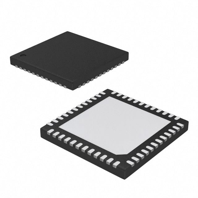
Package and Quantity
The LCMXO2-256HC-5SG48C comes in a 48-pin Small Grid Array (SGA) package. The quantity per package depends on the manufacturer's specifications.
Specifications
- Logic Elements: 256
- Operating Voltage: 1.2V - 3.3V
- I/O Standards: LVCMOS, LVTTL, SSTL
- Package Type: 48-pin SGA
Detailed Pin Configuration
The pin configuration of the LCMXO2-256HC-5SG48C is as follows:
| Pin Number | Pin Name | Description | |------------|----------|-------------| | 1 | VCCIO | I/O Power Supply Voltage | | 2 | GND | Ground | | 3 | IO1 | Input/Output Pin 1 | | 4 | IO2 | Input/Output Pin 2 | | ... | ... | ... | | 48 | IO48 | Input/Output Pin 48 |
Functional Features
- The LCMXO2-256HC-5SG48C provides reconfigurable logic elements that can be programmed to perform various functions.
- It supports internal memory blocks for data storage and processing.
- The FPGA offers flexible I/O capabilities, allowing for easy interfacing with other electronic components.
- It has built-in clock management resources for precise timing control.
Advantages and Disadvantages
Advantages
- High capacity and performance for complex applications.
- Low power consumption, making it suitable for battery-powered devices.
- Reconfigurable nature allows for flexibility in design and prototyping.
- Wide range of supported I/O standards enables compatibility with different systems.
Disadvantages
- Limited availability of alternative models from different manufacturers.
- Steep learning curve for programming and utilizing the full potential of FPGAs.
- Higher cost compared to fixed-function integrated circuits.
Working Principles
FPGAs like the LCMXO2-256HC-5SG48C consist of an array of configurable logic elements interconnected through programmable routing resources. These logic elements can be programmed using a Hardware Description Language (HDL) to implement desired digital logic functions. The configuration data is stored in the internal flash memory of the FPGA.
During operation, the FPGA executes the programmed logic functions based on input signals received through its I/O pins. The output signals are generated by the configured logic elements and routed to the appropriate pins. This flexibility allows for the implementation of complex digital systems on a single chip.
Detailed Application Field Plans
The LCMXO2-256HC-5SG48C can be used in various application fields, including:
- Telecommunications: Implementing signal processing algorithms, protocol converters, and network interfaces.
- Automotive: Controlling engine management systems, driver assistance systems, and infotainment systems.
- Industrial Automation: Building programmable logic controllers (PLCs), motor control systems, and industrial networking devices.
- Consumer Electronics: Designing high-performance audio/video processing, gaming consoles, and smart home automation systems.
Detailed and Complete Alternative Models
While the LCMXO2-256HC-5SG48C is a specific FPGA model, there are alternative models available from different manufacturers that offer similar functionality. Some notable alternatives include:
- Xilinx Spartan-6 XC6SLX9 FPGA
- Intel Cyclone IV EP4CE6E22C8N FPGA
- Microchip PolarFire MPF300TS FPGA
These alternative models provide varying capacities, performance levels, and package options to suit different application requirements.
In conclusion, the LCMXO2-256HC-5SG48C is a high-capacity FPGA with low power consumption and flexible I/O capabilities. It finds applications in diverse fields such as telecommunications, automotive, industrial automation, and consumer electronics. While it has advantages like reconfigurability and high performance
Liệt kê 10 câu hỏi và câu trả lời thường gặp liên quan đến ứng dụng LCMXO2-256HC-5SG48C trong giải pháp kỹ thuật
Sure! Here are 10 common questions and answers related to the application of LCMXO2-256HC-5SG48C in technical solutions:
Q: What is the LCMXO2-256HC-5SG48C? A: The LCMXO2-256HC-5SG48C is a low-cost, low-power FPGA (Field-Programmable Gate Array) device manufactured by Lattice Semiconductor.
Q: What are the key features of LCMXO2-256HC-5SG48C? A: Some key features include 256 LUTs (Look-Up Tables), 2,560 logic cells, 8 multipliers, 4 PLLs (Phase-Locked Loops), and support for various I/O standards.
Q: What are some typical applications of LCMXO2-256HC-5SG48C? A: It is commonly used in applications such as industrial automation, consumer electronics, communication systems, medical devices, and IoT (Internet of Things) solutions.
Q: How can I program the LCMXO2-256HC-5SG48C? A: You can program it using Lattice Diamond or Lattice Radiant software tools, which provide a graphical interface for designing and programming the FPGA.
Q: What are the power requirements for LCMXO2-256HC-5SG48C? A: The device operates at a voltage range of 1.14V to 3.465V, with typical power consumption of around 25mW.
Q: Can I use LCMXO2-256HC-5SG48C for high-speed applications? A: While it may not be suitable for extremely high-speed applications, it can handle moderate-speed designs and is often used in low-power applications.
Q: Does LCMXO2-256HC-5SG48C support external memory interfaces? A: Yes, it supports various memory interfaces such as SPI (Serial Peripheral Interface) and I2C (Inter-Integrated Circuit), allowing you to interface with external memory devices.
Q: Can I use LCMXO2-256HC-5SG48C for real-time signal processing? A: Yes, the device has built-in DSP (Digital Signal Processing) blocks and multipliers, making it suitable for real-time signal processing applications.
Q: Is LCMXO2-256HC-5SG48C suitable for high-reliability applications? A: While it is not specifically designed for high-reliability applications, it can be used in certain scenarios where reliability requirements are not extremely stringent.
Q: Are there any development boards available for LCMXO2-256HC-5SG48C? A: Yes, Lattice Semiconductor provides development boards like the iCE40-HX8K Breakout Board, which allows you to prototype and test your designs using the LCMXO2-256HC-5SG48C FPGA.
Please note that these answers are general and may vary depending on specific design requirements and application scenarios.