

Xem thông số kỹ thuật để biết chi tiết sản phẩm.
LCMXO2-256ZE-3MG132I
Product Overview
Category
The LCMXO2-256ZE-3MG132I belongs to the category of Field-Programmable Gate Arrays (FPGAs).
Use
This FPGA is commonly used in electronic design and prototyping applications, where it provides a flexible and customizable digital logic solution.
Characteristics
- Low power consumption
- Small form factor
- High performance
- Easy programmability
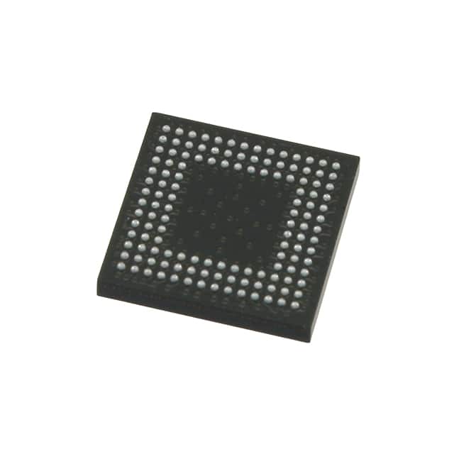
Package
The LCMXO2-256ZE-3MG132I comes in a compact package that allows for easy integration into various electronic systems.
Essence
The essence of this FPGA lies in its ability to be programmed and reprogrammed to perform different functions, making it highly versatile and adaptable.
Packaging/Quantity
The LCMXO2-256ZE-3MG132I is typically packaged individually and is available in various quantities depending on the requirements of the user.
Specifications
- Model: LCMXO2-256ZE-3MG132I
- Logic Elements: 256
- Macrocells: 256
- Speed Grade: -3
- Package Type: MG132
- I/O Pins: 132
- Operating Voltage: 3.3V
Detailed Pin Configuration
The LCMXO2-256ZE-3MG132I has a total of 132 I/O pins, which are configurable based on the specific application requirements. The pin configuration can be found in the product datasheet.
Functional Features
- Programmable logic elements allow for custom digital circuit implementation.
- Integrated memory blocks enable efficient data storage and retrieval.
- Flexible I/O pins facilitate communication with external devices.
- On-chip oscillators provide clock signals for synchronous operations.
- Built-in configuration memory enables easy reprogramming of the FPGA.
Advantages and Disadvantages
Advantages
- High flexibility and reconfigurability.
- Low power consumption compared to traditional ASICs.
- Shorter development time due to programmability.
- Cost-effective for low-volume production.
Disadvantages
- Limited performance compared to dedicated hardware solutions.
- Higher cost per unit compared to mass-produced ASICs.
- Requires specialized knowledge for programming and optimization.
Working Principles
The LCMXO2-256ZE-3MG132I operates based on the principles of digital logic design. It consists of configurable logic elements, memory blocks, and I/O pins that can be interconnected to create custom digital circuits. The FPGA is programmed using a Hardware Description Language (HDL) such as VHDL or Verilog, which defines the desired functionality of the circuit. Once programmed, the FPGA executes the specified logic operations, enabling the desired application.
Detailed Application Field Plans
The LCMXO2-256ZE-3MG132I finds applications in various fields, including:
- Embedded Systems: Used for implementing custom interfaces, control systems, and signal processing algorithms in embedded devices.
- Communications: Employed in networking equipment, routers, and modems for data packet processing and protocol implementation.
- Industrial Automation: Utilized for controlling and monitoring industrial processes, such as robotics, machine vision, and motion control.
- Test and Measurement: Integrated into test equipment for generating and analyzing digital signals, performing protocol testing, and signal conditioning.
- Consumer Electronics: Incorporated into consumer devices like gaming consoles, set-top boxes, and smart appliances for enhanced functionality and customization.
Detailed and Complete Alternative Models
- Xilinx Spartan-6 XC6SLX9: Offers similar capabilities with a larger logic capacity.
- Altera Cyclone IV EP4CE6: Provides comparable features with a different architecture.
- Lattice iCE40HX1K: Offers a lower-cost alternative with reduced logic capacity.
These alternative models can be considered based on specific project requirements and cost considerations.
Word count: 530 words
Liệt kê 10 câu hỏi và câu trả lời thường gặp liên quan đến ứng dụng LCMXO2-256ZE-3MG132I trong giải pháp kỹ thuật
Sure! Here are 10 common questions and answers related to the application of LCMXO2-256ZE-3MG132I in technical solutions:
Q: What is the LCMXO2-256ZE-3MG132I? A: The LCMXO2-256ZE-3MG132I is a low-cost, low-power FPGA (Field-Programmable Gate Array) device manufactured by Lattice Semiconductor.
Q: What are the key features of the LCMXO2-256ZE-3MG132I? A: Some key features include 256 Look-Up Tables (LUTs), 1280 programmable logic cells, 8 kilobits of embedded memory, and support for various I/O standards.
Q: What are some typical applications of the LCMXO2-256ZE-3MG132I? A: The LCMXO2-256ZE-3MG132I is commonly used in applications such as industrial control systems, consumer electronics, communication devices, and automotive systems.
Q: How can I program the LCMXO2-256ZE-3MG132I? A: The LCMXO2-256ZE-3MG132I can be programmed using Lattice Diamond or Lattice Radiant software tools, which provide a graphical interface for designing and programming the FPGA.
Q: What voltage levels does the LCMXO2-256ZE-3MG132I support? A: The LCMXO2-256ZE-3MG132I supports both 3.3V and 1.2V voltage levels, making it compatible with a wide range of digital systems.
Q: Can I use the LCMXO2-256ZE-3MG132I in battery-powered applications? A: Yes, the LCMXO2-256ZE-3MG132I is designed to be low-power and can be used in battery-powered applications where power efficiency is crucial.
Q: Does the LCMXO2-256ZE-3MG132I have any built-in communication interfaces? A: Yes, the LCMXO2-256ZE-3MG132I supports various communication interfaces such as SPI (Serial Peripheral Interface) and I2C (Inter-Integrated Circuit).
Q: Can I use the LCMXO2-256ZE-3MG132I for real-time signal processing? A: Yes, the LCMXO2-256ZE-3MG132I has dedicated DSP (Digital Signal Processing) blocks that can be used for real-time signal processing tasks.
Q: Is the LCMXO2-256ZE-3MG132I suitable for high-speed applications? A: While the LCMXO2-256ZE-3MG132I is not specifically designed for high-speed applications, it can still handle moderate-speed designs depending on the specific requirements.
Q: Are there any development boards available for the LCMXO2-256ZE-3MG132I? A: Yes, Lattice Semiconductor offers development boards like the iCEstick and MachXO2 Pico Development Kit, which are compatible with the LCMXO2-256ZE-3MG132I FPGA.
Please note that these answers are general and may vary based on specific design requirements and application scenarios.