

Xem thông số kỹ thuật để biết chi tiết sản phẩm.
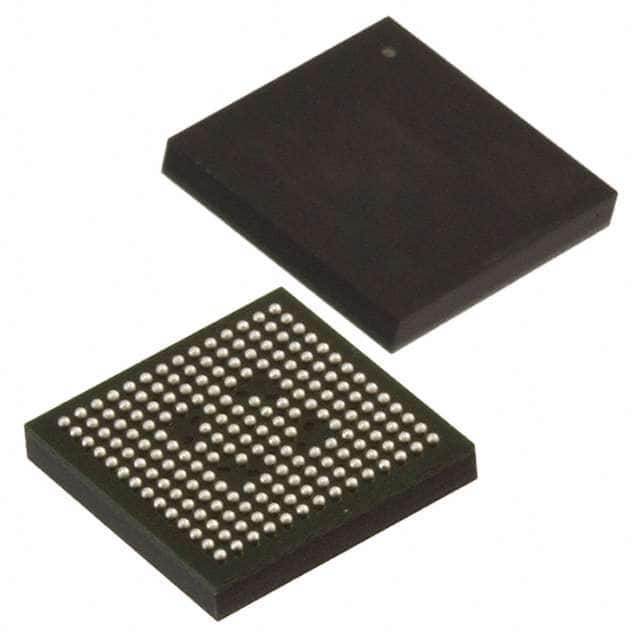
LCMXO2-4000HE-4MG184C
Product Overview
Category
The LCMXO2-4000HE-4MG184C belongs to the category of Field-Programmable Gate Arrays (FPGAs).
Use
FPGAs are integrated circuits that can be programmed and reprogrammed to perform various digital functions. The LCMXO2-4000HE-4MG184C is specifically designed for applications requiring low power consumption and high performance.
Characteristics
- Low power consumption: The LCMXO2-4000HE-4MG184C is optimized for power efficiency, making it suitable for battery-powered devices.
- High performance: With a high logic density and fast processing capabilities, this FPGA can handle complex tasks efficiently.
- Small package size: The LCMXO2-4000HE-4MG184C comes in a compact package, making it ideal for space-constrained designs.
- Enhanced security features: This FPGA offers built-in security mechanisms to protect sensitive data.
Package and Quantity
The LCMXO2-4000HE-4MG184C is available in a 184-pin Micro FineLine BGA (uBGA) package. It is typically sold individually or in small quantities.
Specifications
- Logic Cells: 4000
- Look-Up Tables (LUTs): 4000
- Flip-Flops: 8000
- Block RAM: 112 Kbits
- Maximum Operating Frequency: 150 MHz
- I/O Pins: 184
- Voltage Range: 1.14V - 1.26V
- Operating Temperature Range: -40°C to 85°C
Detailed Pin Configuration
The LCMXO2-4000HE-4MG184C has 184 pins, each serving a specific purpose. The pin configuration includes dedicated input/output pins, power supply pins, and configuration pins. A detailed pinout diagram can be found in the product datasheet.
Functional Features
- Programmability: The LCMXO2-4000HE-4MG184C can be programmed using Hardware Description Languages (HDL) such as VHDL or Verilog.
- Reconfigurability: The FPGA can be reprogrammed multiple times, allowing for flexibility in design changes or updates.
- I/O Flexibility: The device offers a wide range of I/O options, including LVCMOS, LVTTL, and differential signaling standards.
- Embedded Memory: The built-in Block RAM provides fast and efficient memory storage for data-intensive applications.
- Clock Management: The FPGA supports various clocking options, including PLLs and DLLs, enabling precise timing control.
Advantages and Disadvantages
Advantages
- Low power consumption makes it suitable for portable and battery-powered devices.
- High logic density allows for complex designs and efficient resource utilization.
- Reconfigurability enables flexibility in adapting to changing requirements.
- Enhanced security features protect sensitive data from unauthorized access.
Disadvantages
- Limited availability in large quantities due to its small package size.
- Higher cost compared to other non-programmable integrated circuits.
- Steeper learning curve for programming and utilizing FPGAs compared to traditional microcontrollers.
Working Principles
The LCMXO2-4000HE-4MG184C operates based on the principles of digital logic. It consists of configurable logic blocks interconnected through programmable routing resources. The device is programmed to implement desired logic functions by configuring the interconnections and functionality of these blocks.
Detailed Application Field Plans
The LCMXO2-4000HE-4MG184C finds applications in various fields, including:
- Embedded Systems: It can be used in the development of embedded systems, such as industrial control systems and IoT devices.
- Communications: The FPGA can be employed in communication systems for signal processing, encryption/decryption, and protocol implementation.
- Image and Video Processing: It is suitable for image and video processing applications, including real-time video streaming, image recognition, and computer vision.
- Test and Measurement Equipment: The FPGA can be utilized in test and measurement equipment for signal generation, data acquisition, and protocol analysis.
Detailed and Complete Alternative Models
- Xilinx Spartan-6 XC6SLX9: A comparable FPGA with similar logic capacity and performance characteristics.
- Intel Cyclone IV EP4CE22: An alternative FPGA offering a balance between cost and performance.
- Lattice iCE40UP5K: A low-power FPGA with a smaller logic capacity but suitable for battery-powered applications.
These alternative models provide options based on specific requirements and constraints.
In conclusion, the LCMXO2-4000HE-4MG184C is a versatile FPGA that combines low power consumption, high performance, and compact size.
Liệt kê 10 câu hỏi và câu trả lời thường gặp liên quan đến ứng dụng LCMXO2-4000HE-4MG184C trong giải pháp kỹ thuật
Sure! Here are 10 common questions and answers related to the application of LCMXO2-4000HE-4MG184C in technical solutions:
Q: What is the LCMXO2-4000HE-4MG184C? A: The LCMXO2-4000HE-4MG184C is a low-cost, low-power FPGA (Field-Programmable Gate Array) device manufactured by Lattice Semiconductor.
Q: What are the key features of the LCMXO2-4000HE-4MG184C? A: Some key features include 4000 Look-Up Tables (LUTs), 128 Kbits of embedded block RAM, 34 I/O pins, and support for various I/O standards.
Q: What are some typical applications of the LCMXO2-4000HE-4MG184C? A: The LCMXO2-4000HE-4MG184C is commonly used in applications such as industrial control systems, consumer electronics, medical devices, and communication equipment.
Q: How can I program the LCMXO2-4000HE-4MG184C? A: The LCMXO2-4000HE-4MG184C can be programmed using Lattice Diamond or Lattice Radiant software tools, which provide a graphical interface for designing and programming the FPGA.
Q: What voltage levels does the LCMXO2-4000HE-4MG184C support? A: The LCMXO2-4000HE-4MG184C supports both 3.3V and 1.2V voltage levels, making it compatible with a wide range of digital logic circuits.
Q: Can I use the LCMXO2-4000HE-4MG184C in battery-powered devices? A: Yes, the LCMXO2-4000HE-4MG184C is designed to be low-power and can be used in battery-powered devices where power consumption is a concern.
Q: Does the LCMXO2-4000HE-4MG184C support external memory interfaces? A: Yes, the LCMXO2-4000HE-4MG184C has dedicated pins for interfacing with external memory devices such as SRAM or SDRAM.
Q: Can I use the LCMXO2-4000HE-4MG184C for high-speed communication protocols? A: Yes, the LCMXO2-4000HE-4MG184C supports various high-speed communication protocols like SPI, I2C, UART, and LVDS.
Q: Is the LCMXO2-4000HE-4MG184C suitable for complex digital signal processing (DSP) algorithms? A: While the LCMXO2-4000HE-4MG184C does have some DSP capabilities, it is more commonly used for general-purpose logic functions rather than complex DSP algorithms.
Q: Where can I find additional resources and support for the LCMXO2-4000HE-4MG184C? A: You can find datasheets, application notes, and technical support on the official Lattice Semiconductor website or by contacting their customer support team.