

Xem thông số kỹ thuật để biết chi tiết sản phẩm.
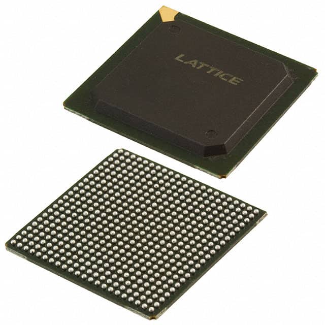
LCMXO2-7000ZE-2FG484I
Product Overview
Category
The LCMXO2-7000ZE-2FG484I belongs to the category of Field-Programmable Gate Arrays (FPGAs).
Use
FPGAs are integrated circuits that can be programmed and reprogrammed to perform various digital functions. The LCMXO2-7000ZE-2FG484I is specifically designed for applications requiring low power consumption and high performance.
Characteristics
- Low power consumption: The LCMXO2-7000ZE-2FG484I is optimized for low-power operation, making it suitable for battery-powered devices.
- High performance: With a high logic density and advanced architecture, this FPGA offers excellent performance for complex digital designs.
- Small package size: The device comes in a compact FG484 package, allowing for space-efficient integration into electronic systems.
- Easy programming: The LCMXO2-7000ZE-2FG484I can be programmed using popular hardware description languages (HDLs) such as VHDL or Verilog.
Package and Quantity
The LCMXO2-7000ZE-2FG484I is available in a Fine-Pitch Ball Grid Array (FBGA) package with 484 pins. It is typically sold individually or in small quantities for prototyping and small-scale production.
Specifications
- Logic Cells: 7,000
- Look-Up Tables (LUTs): 4,500
- Flip-Flops: 8,000
- Block RAM: 112 Kbits
- Maximum User I/Os: 266
- Operating Voltage: 1.2V
- Speed Grade: -2 (Industrial)
Detailed Pin Configuration
The LCMXO2-7000ZE-2FG484I has a total of 484 pins, each serving a specific purpose in the device's operation. The pin configuration includes input/output pins, power supply pins, clock pins, and configuration pins. A detailed pinout diagram can be found in the product datasheet.
Functional Features
- Programmable Logic: The FPGA provides a flexible and customizable logic fabric that allows users to implement their desired digital circuits.
- I/O Interfaces: The LCMXO2-7000ZE-2FG484I supports various standard interfaces such as GPIO, SPI, I2C, UART, and more, enabling seamless integration with external devices.
- Embedded Memory: The built-in block RAM provides on-chip memory resources for data storage and retrieval, enhancing the overall performance of the system.
- Clock Management: The FPGA offers dedicated clock management resources, including phase-locked loops (PLLs) and delay-locked loops (DLLs), ensuring precise timing control.
Advantages and Disadvantages
Advantages
- Low power consumption makes it suitable for battery-powered applications.
- High logic density enables complex designs to be implemented efficiently.
- Easy programming using popular HDLs simplifies development.
- Compact package size allows for space-efficient integration.
Disadvantages
- Limited number of user I/Os may restrict connectivity options in certain applications.
- Advanced features and capabilities may require a steeper learning curve for inexperienced users.
Working Principles
The LCMXO2-7000ZE-2FG484I operates based on the principles of reconfigurable computing. It consists of an array of configurable logic blocks interconnected through programmable routing resources. Users can program the FPGA by specifying the desired interconnections and functionality of the logic blocks using a hardware description language. Once programmed, the FPGA executes the specified digital circuitry.
Detailed Application Field Plans
The LCMXO2-7000ZE-2FG484I finds applications in various fields, including:
- Embedded Systems: The FPGA can be used to implement custom interfaces, control systems, and signal processing algorithms in embedded devices.
- Communications: It can be utilized for protocol conversion, data encryption/decryption, and signal modulation/demodulation in communication systems.
- Industrial Automation: The FPGA enables the implementation of real-time control systems, motor control, and sensor interfacing in industrial automation applications.
- Medical Devices: It can be employed for medical imaging, patient monitoring, and diagnostic equipment, leveraging its high-performance capabilities.
- Aerospace and Defense: The FPGA is suitable for radar systems, avionics, secure communications, and image processing in aerospace and defense applications.
Detailed and Complete Alternative Models
- LCMXO2-1200ZE-1TG144C
- LCMXO2-2000HC-4BG256C
- LCMXO2-4000HE-6MG132C
- LCMXO2-7000HC-4SG48C
These alternative models offer different logic capacities, package options, and performance
Liệt kê 10 câu hỏi và câu trả lời thường gặp liên quan đến ứng dụng LCMXO2-7000ZE-2FG484I trong giải pháp kỹ thuật
Sure! Here are 10 common questions and answers related to the application of LCMXO2-7000ZE-2FG484I in technical solutions:
Q: What is the LCMXO2-7000ZE-2FG484I? A: The LCMXO2-7000ZE-2FG484I is a low-cost, low-power FPGA (Field-Programmable Gate Array) device manufactured by Lattice Semiconductor.
Q: What are the key features of the LCMXO2-7000ZE-2FG484I? A: Some key features include 7000 Look-Up Tables (LUTs), 128 Kbits of embedded block RAM, 34 I/O pins, and support for various I/O standards.
Q: What are some typical applications of the LCMXO2-7000ZE-2FG484I? A: The LCMXO2-7000ZE-2FG484I is commonly used in applications such as industrial control systems, consumer electronics, communication devices, and automotive systems.
Q: How can I program the LCMXO2-7000ZE-2FG484I? A: The LCMXO2-7000ZE-2FG484I can be programmed using Lattice Diamond or Lattice Radiant software tools, which support various programming languages like VHDL and Verilog.
Q: What is the power consumption of the LCMXO2-7000ZE-2FG484I? A: The power consumption of the LCMXO2-7000ZE-2FG484I depends on the design and utilization of the FPGA, but it is generally known for its low-power characteristics.
Q: Can I use the LCMXO2-7000ZE-2FG484I in battery-powered devices? A: Yes, the low-power consumption of the LCMXO2-7000ZE-2FG484I makes it suitable for battery-powered devices where power efficiency is crucial.
Q: What are the I/O voltage levels supported by the LCMXO2-7000ZE-2FG484I? A: The LCMXO2-7000ZE-2FG484I supports various I/O voltage standards, including 1.2V, 1.5V, 1.8V, 2.5V, and 3.3V.
Q: Can I interface the LCMXO2-7000ZE-2FG484I with other components or microcontrollers? A: Yes, the LCMXO2-7000ZE-2FG484I can be easily interfaced with other components or microcontrollers using its I/O pins and supported communication protocols.
Q: Is the LCMXO2-7000ZE-2FG484I suitable for high-speed applications? A: While the LCMXO2-7000ZE-2FG484I is not specifically designed for high-speed applications, it can still handle moderate-speed designs effectively.
Q: Where can I find more information about the LCMXO2-7000ZE-2FG484I? A: You can find more detailed information about the LCMXO2-7000ZE-2FG484I in the datasheet provided by Lattice Semiconductor or on their official website.