

Xem thông số kỹ thuật để biết chi tiết sản phẩm.
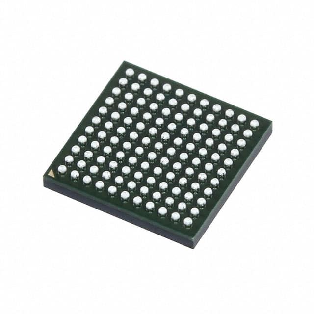
LCMXO3LF-1300E-6MG121I
Product Overview
Category
The LCMXO3LF-1300E-6MG121I belongs to the category of Field Programmable Gate Arrays (FPGAs).
Use
FPGAs are integrated circuits that can be programmed and reprogrammed to perform various digital functions. The LCMXO3LF-1300E-6MG121I is specifically designed for applications requiring high-performance and low-power consumption.
Characteristics
- High performance: The LCMXO3LF-1300E-6MG121I offers a high logic density and fast processing capabilities, making it suitable for complex digital designs.
- Low power consumption: This FPGA is optimized for power efficiency, allowing for longer battery life in portable devices.
- Small package size: The LCMXO3LF-1300E-6MG121I comes in a compact package, making it suitable for space-constrained applications.
- Robust design: It features built-in security features and reliable operation, ensuring the integrity and safety of the digital system.
Package and Quantity
The LCMXO3LF-1300E-6MG121I is available in a surface-mount package. The exact dimensions and pin configuration can be found in the specifications section below. It is typically sold in quantities of one or more, depending on the requirements of the application.
Specifications
- Logic Elements: 1,300
- Look-Up Tables (LUTs): 3,900
- Flip-Flops: 2,600
- Block RAM: 72 Kbits
- Maximum Operating Frequency: 250 MHz
- I/O Pins: 121
- Voltage Range: 1.14V - 1.26V
- Package Type: QFN
- Package Dimensions: 8mm x 8mm
Pin Configuration
The LCMXO3LF-1300E-6MG121I has a total of 121 I/O pins. The detailed pin configuration can be found in the manufacturer's datasheet.
Functional Features
- High-speed processing: The FPGA offers fast data processing capabilities, enabling real-time applications.
- Flexible reconfiguration: It can be programmed and reprogrammed to adapt to changing requirements or to implement different functionalities.
- Embedded memory: The built-in block RAM allows for efficient storage and retrieval of data.
- I/O flexibility: The FPGA provides a wide range of I/O options, allowing for seamless integration with other components or systems.
- Security features: It includes security mechanisms to protect against unauthorized access or tampering.
Advantages and Disadvantages
Advantages
- High performance and low power consumption make it suitable for a wide range of applications.
- Compact package size enables use in space-constrained designs.
- Flexible reconfiguration allows for versatility and adaptability.
- Built-in security features enhance system integrity and safety.
Disadvantages
- Limited logic elements and resources compared to larger FPGAs.
- Higher cost per logic element compared to some alternatives.
- Steeper learning curve for programming and utilizing the FPGA's full potential.
Working Principles
The LCMXO3LF-1300E-6MG121I operates based on the principles of digital logic. It consists of configurable logic blocks (CLBs), interconnects, and I/O elements. The CLBs contain look-up tables (LUTs) that can be programmed to implement desired logic functions. The interconnects provide routing paths between the CLBs, allowing for the flow of data. The I/O elements enable communication with external devices.
Upon programming, the FPGA's internal configuration memory is set, defining the desired functionality. The input signals are processed through the CLBs, and the output signals are routed to the appropriate I/O pins. The FPGA can be reprogrammed as needed to modify or update the implemented logic.
Detailed Application Field Plans
The LCMXO3LF-1300E-6MG121I finds applications in various fields, including:
- Communications: It can be used in wireless communication systems, network routers, and data transmission equipment.
- Industrial automation: The FPGA is suitable for controlling and monitoring industrial processes, robotics, and machine vision systems.
- Automotive electronics: It can be utilized in automotive control units, driver assistance systems, and infotainment systems.
- Medical devices: The FPGA can be integrated into medical imaging equipment, patient monitoring systems, and diagnostic instruments.
- Aerospace and defense: It finds applications in radar systems, avionics, unmanned aerial vehicles (UAVs), and secure communication systems.
Alternative Models
For those seeking alternative options, the following FPGAs can be considered:
- LCMXO2-1200ZE-1TG144C
- LCMXO4L
Liệt kê 10 câu hỏi và câu trả lời thường gặp liên quan đến ứng dụng LCMXO3LF-1300E-6MG121I trong giải pháp kỹ thuật
Sure! Here are 10 common questions and answers related to the application of LCMXO3LF-1300E-6MG121I in technical solutions:
Q: What is the LCMXO3LF-1300E-6MG121I? A: The LCMXO3LF-1300E-6MG121I is a specific model of Field-Programmable Gate Array (FPGA) manufactured by Lattice Semiconductor.
Q: What are the key features of the LCMXO3LF-1300E-6MG121I? A: Some key features include low power consumption, small form factor, high-performance logic fabric, and embedded memory blocks.
Q: What are the typical applications of the LCMXO3LF-1300E-6MG121I? A: The LCMXO3LF-1300E-6MG121I is commonly used in various technical solutions such as industrial automation, consumer electronics, automotive systems, and communication devices.
Q: How can I program the LCMXO3LF-1300E-6MG121I? A: The LCMXO3LF-1300E-6MG121I can be programmed using hardware description languages (HDLs) like VHDL or Verilog, along with specialized software tools provided by Lattice Semiconductor.
Q: What is the power supply requirement for the LCMXO3LF-1300E-6MG121I? A: The LCMXO3LF-1300E-6MG121I typically operates on a voltage supply range of 1.14V to 1.26V.
Q: Can I use the LCMXO3LF-1300E-6MG121I in battery-powered devices? A: Yes, the low power consumption of the LCMXO3LF-1300E-6MG121I makes it suitable for battery-powered applications.
Q: Does the LCMXO3LF-1300E-6MG121I support external memory interfaces? A: Yes, the LCMXO3LF-1300E-6MG121I supports various memory interfaces such as DDR3, DDR2, and SPI Flash.
Q: Can I use the LCMXO3LF-1300E-6MG121I for real-time signal processing? A: Yes, the high-performance logic fabric of the LCMXO3LF-1300E-6MG121I enables real-time signal processing capabilities.
Q: Are there any development boards available for the LCMXO3LF-1300E-6MG121I? A: Yes, Lattice Semiconductor provides development boards like the LCMXO3L-EVN for prototyping and evaluation purposes.
Q: Where can I find technical documentation and support for the LCMXO3LF-1300E-6MG121I? A: You can find technical documentation, datasheets, application notes, and support resources on the official website of Lattice Semiconductor or by contacting their customer support team.