

Xem thông số kỹ thuật để biết chi tiết sản phẩm.
LCMXO3LF-2100E-5UWG49ITR1K
Product Overview
Category
The LCMXO3LF-2100E-5UWG49ITR1K belongs to the category of Field Programmable Gate Arrays (FPGAs).
Use
FPGAs are integrated circuits that can be programmed after manufacturing. The LCMXO3LF-2100E-5UWG49ITR1K is specifically designed for use in electronic systems where flexibility and reconfigurability are required.
Characteristics
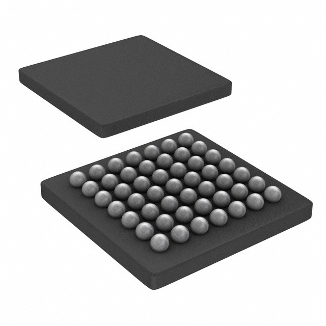
- Package: The LCMXO3LF-2100E-5UWG49ITR1K comes in a compact package suitable for surface mount technology.
- Essence: This FPGA offers a high level of integration, allowing for complex digital logic designs.
- Packaging/Quantity: The LCMXO3LF-2100E-5UWG49ITR1K is typically sold in reels or trays, with a quantity of 250 units per reel/tray.
Specifications
- Logic Cells: 2100
- Operating Voltage: 1.2V
- Speed Grade: -5
- I/O Pins: 49
- Temperature Range: Industrial (-40°C to +85°C)
- RoHS Compliance: Yes
Detailed Pin Configuration
The LCMXO3LF-2100E-5UWG49ITR1K has a total of 49 I/O pins. These pins are used for input/output connections with other components in the system. The pin configuration is as follows:
- Pin 1: VCCIO
- Pin 2: GND
- Pin 3: IO_0
- Pin 4: IO_1
- ...
- Pin 49: IO_48
Functional Features
- High Flexibility: The LCMXO3LF-2100E-5UWG49ITR1K allows for on-the-fly reconfiguration, enabling rapid prototyping and design changes.
- Low Power Consumption: This FPGA is designed to operate efficiently, minimizing power consumption in electronic systems.
- High Performance: With 2100 logic cells, the LCMXO3LF-2100E-5UWG49ITR1K offers a high level of performance for complex digital designs.
Advantages and Disadvantages
Advantages
- Flexibility and reconfigurability
- Low power consumption
- High integration level
- Suitable for rapid prototyping
Disadvantages
- Limited number of I/O pins
- May require specialized programming knowledge
Working Principles
FPGAs like the LCMXO3LF-2100E-5UWG49ITR1K consist of an array of configurable logic blocks (CLBs) interconnected by programmable interconnects. These CLBs can be programmed to implement various digital logic functions, allowing for the creation of complex circuits. The configuration of the FPGA is stored in non-volatile memory and can be modified as needed.
Detailed Application Field Plans
The LCMXO3LF-2100E-5UWG49ITR1K finds applications in various fields, including:
- Embedded Systems: It can be used in embedded systems for controlling and interfacing with other components.
- Communications: The FPGA can be utilized in communication systems for signal processing and protocol implementation.
- Industrial Automation: It can be employed in industrial automation systems for control and monitoring purposes.
- Medical Devices: The LCMXO3LF-2100E-5UWG49ITR1K can be integrated into medical devices for data acquisition and processing.
Detailed and Complete Alternative Models
- LCMXO2LF-1200E-5UWG49ITR1K
- LCMXO3LF-4300E-5UWG49ITR1K
- LCMXO3LF-6900E-5UWG49ITR1K
- LCMXO3LF-9400E-5UWG49ITR1K
These alternative models offer different logic cell counts and I/O pin configurations, providing options to suit specific design requirements.
Word count: 402 words
Liệt kê 10 câu hỏi và câu trả lời thường gặp liên quan đến ứng dụng LCMXO3LF-2100E-5UWG49ITR1K trong giải pháp kỹ thuật
Sure! Here are 10 common questions and answers related to the application of LCMXO3LF-2100E-5UWG49ITR1K in technical solutions:
Q1: What is the LCMXO3LF-2100E-5UWG49ITR1K? A1: The LCMXO3LF-2100E-5UWG49ITR1K is a specific model of Field-Programmable Gate Array (FPGA) manufactured by Lattice Semiconductor.
Q2: What is an FPGA? A2: FPGA stands for Field-Programmable Gate Array. It is a type of integrated circuit that can be programmed or reconfigured after manufacturing to perform specific functions.
Q3: What are the key features of the LCMXO3LF-2100E-5UWG49ITR1K? A3: Some key features of the LCMXO3LF-2100E-5UWG49ITR1K include low power consumption, small form factor, high logic density, and support for various I/O standards.
Q4: What are the typical applications of the LCMXO3LF-2100E-5UWG49ITR1K? A4: The LCMXO3LF-2100E-5UWG49ITR1K is commonly used in applications such as industrial automation, automotive electronics, consumer electronics, telecommunications, and Internet of Things (IoT) devices.
Q5: How can the LCMXO3LF-2100E-5UWG49ITR1K be programmed? A5: The LCMXO3LF-2100E-5UWG49ITR1K can be programmed using Hardware Description Languages (HDLs) such as VHDL or Verilog, which describe the desired functionality of the FPGA.
Q6: What development tools are available for working with the LCMXO3LF-2100E-5UWG49ITR1K? A6: Lattice Semiconductor provides a range of development tools, including the Lattice Diamond design software and the Lattice Radiant software, which can be used to program and configure the LCMXO3LF-2100E-5UWG49ITR1K.
Q7: Can the LCMXO3LF-2100E-5UWG49ITR1K interface with other components or devices? A7: Yes, the LCMXO3LF-2100E-5UWG49ITR1K supports various I/O standards, allowing it to interface with other components or devices such as sensors, displays, memory modules, and communication interfaces.
Q8: What is the power consumption of the LCMXO3LF-2100E-5UWG49ITR1K? A8: The LCMXO3LF-2100E-5UWG49ITR1K is designed to have low power consumption, making it suitable for battery-powered or energy-efficient applications. The exact power consumption depends on the specific design and usage scenario.
Q9: Can the LCMXO3LF-2100E-5UWG49ITR1K be reprogrammed multiple times? A9: Yes, the LCMXO3LF-2100E-5UWG49ITR1K is a reprogrammable FPGA, meaning it can be programmed and reconfigured multiple times to implement different functionalities or updates.
Q10: Are there any limitations or considerations when using the LCMXO3LF-2100E-5UWG49ITR1K? A10: Some considerations when using the LCMXO3LF-2100E-5UWG49ITR1K include understanding the specific requirements of your application, ensuring compatibility with other components or devices, and optimizing the design for power consumption and performance. It is also important to refer to the manufacturer's documentation and guidelines for proper usage.