

Xem thông số kỹ thuật để biết chi tiết sản phẩm.
LCMXO3LF-4300C-5BG400I
Product Overview
Category
The LCMXO3LF-4300C-5BG400I belongs to the category of Field-Programmable Gate Arrays (FPGAs).
Use
FPGAs are integrated circuits that can be programmed after manufacturing, allowing for flexible and customizable digital logic designs. The LCMXO3LF-4300C-5BG400I is specifically designed for applications requiring high-performance and low-power consumption.
Characteristics
- High performance: The LCMXO3LF-4300C-5BG400I offers a high-speed processing capability, making it suitable for demanding applications.
- Low power consumption: This FPGA is designed to minimize power consumption, making it energy-efficient.
- Compact package: The LCMXO3LF-4300C-5BG400I comes in a compact package, enabling space-saving integration into various electronic systems.
- Versatile functionality: It provides a wide range of features and functions, allowing for diverse application possibilities.
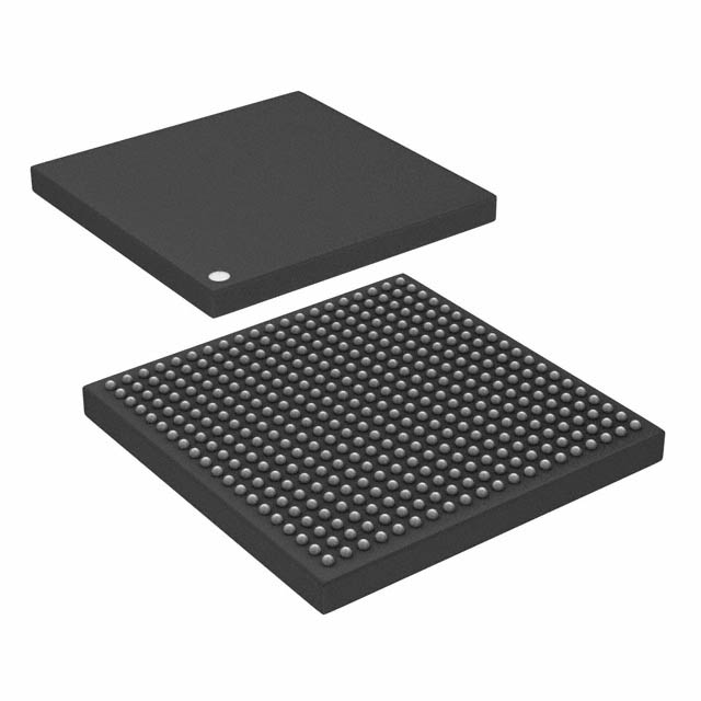
Package and Quantity
The LCMXO3LF-4300C-5BG400I is available in a BG400 package. Each package contains one unit of the FPGA.
Specifications
- Device family: LatticeECP3
- Logic elements: 43,008
- Embedded memory: 4,608 Kbits
- User I/Os: 332
- Operating voltage: 1.2V
- Maximum operating frequency: 400 MHz
- Package type: Ball Grid Array (BGA)
- Package dimensions: 17mm x 17mm
Detailed Pin Configuration
The LCMXO3LF-4300C-5BG400I has a total of 332 user I/O pins. These pins can be configured to perform various functions based on the specific application requirements. A detailed pin configuration diagram and description can be found in the product datasheet.
Functional Features
- High-speed processing: The FPGA offers fast data processing capabilities, enabling real-time applications.
- Flexible design: It allows for reprogramming of the logic circuitry, making it adaptable to changing requirements.
- Configurable I/Os: The user I/O pins can be configured as inputs or outputs, supporting versatile interfacing options.
- Embedded memory: The FPGA includes a significant amount of embedded memory, facilitating efficient data storage and retrieval.
- Built-in DSP blocks: It features dedicated digital signal processing (DSP) blocks, enhancing performance for signal processing applications.
Advantages and Disadvantages
Advantages
- Customizability: FPGAs provide the ability to create custom logic designs tailored to specific application needs.
- High performance: The LCMXO3LF-4300C-5BG400I offers high-speed processing capabilities suitable for demanding applications.
- Low power consumption: It is designed to minimize power usage, resulting in energy-efficient operation.
- Versatility: The FPGA's flexible nature allows for a wide range of applications and functionalities.
Disadvantages
- Complexity: Working with FPGAs requires specialized knowledge and expertise in digital design and programming.
- Cost: FPGAs can be more expensive compared to other integrated circuits due to their programmable nature and advanced features.
- Limited scalability: FPGAs have a fixed number of logic elements and I/O pins, which may limit scalability for certain applications.
Working Principles
FPGAs consist of an array of configurable logic blocks (CLBs) interconnected by programmable routing resources. The LCMXO3LF-4300C-5BG400I utilizes look-up tables (LUTs) within the CLBs to implement desired logic functions. These LUTs can be programmed to create complex digital circuits. The interconnections between CLBs are established using programmable routing resources, allowing for the desired signal flow.
Detailed Application Field Plans
The LCMXO3LF-4300C-5BG400I finds applications in various fields, including but not limited to: - Communications: It can be used in wireless communication systems, network routers, and data transmission equipment. - Industrial automation: The FPGA enables control and monitoring of industrial processes, robotics, and machine vision systems. - Aerospace and defense: It is suitable for radar systems, avionics, and secure communication systems. - Medical devices: The FPGA can be utilized in medical imaging, patient monitoring, and diagnostic equipment. - Automotive electronics: It supports advanced driver assistance systems (ADAS), infotainment systems, and engine control units.
Detailed and Complete Alternative Models
- LCMXO2-1200ZE-1TG100C
- XC7A35T-1CPG236C
- EP4CE6E22C8N
- MAX 10M08SAU169C8G
These alternative models
Liệt kê 10 câu hỏi và câu trả lời thường gặp liên quan đến ứng dụng LCMXO3LF-4300C-5BG400I trong giải pháp kỹ thuật
Sure! Here are 10 common questions and answers related to the application of LCMXO3LF-4300C-5BG400I in technical solutions:
Q: What is the LCMXO3LF-4300C-5BG400I? A: The LCMXO3LF-4300C-5BG400I is a low-power, small form factor FPGA (Field-Programmable Gate Array) device manufactured by Lattice Semiconductor.
Q: What are the key features of the LCMXO3LF-4300C-5BG400I? A: Some key features include low power consumption, small package size, high logic density, and support for various I/O standards.
Q: What are the typical applications of LCMXO3LF-4300C-5BG400I? A: The LCMXO3LF-4300C-5BG400I is commonly used in applications such as industrial automation, consumer electronics, IoT devices, and embedded systems.
Q: How can I program the LCMXO3LF-4300C-5BG400I? A: The LCMXO3LF-4300C-5BG400I can be programmed using Lattice Diamond or Lattice Radiant software tools, which support various programming languages like VHDL and Verilog.
Q: What is the power supply requirement for LCMXO3LF-4300C-5BG400I? A: The LCMXO3LF-4300C-5BG400I typically operates at a voltage range of 1.14V to 1.26V, with a maximum power consumption of around 100mW.
Q: Can I use the LCMXO3LF-4300C-5BG400I in battery-powered devices? A: Yes, the low power consumption of the LCMXO3LF-4300C-5BG400I makes it suitable for battery-powered applications where power efficiency is crucial.
Q: What are the available I/O interfaces on the LCMXO3LF-4300C-5BG400I? A: The LCMXO3LF-4300C-5BG400I provides a variety of I/O standards, including LVCMOS, LVTTL, and LVDS, allowing for easy integration with other components.
Q: Can I use the LCMXO3LF-4300C-5BG400I for high-speed data processing? A: While the LCMXO3LF-4300C-5BG400I is not specifically designed for high-speed data processing, it can handle moderate data rates depending on the complexity of the design.
Q: Are there any development boards or evaluation kits available for the LCMXO3LF-4300C-5BG400I? A: Yes, Lattice Semiconductor offers development boards and evaluation kits that include the LCMXO3LF-4300C-5BG400I, allowing users to quickly prototype their designs.
Q: Where can I find technical documentation and support for the LCMXO3LF-4300C-5BG400I? A: Technical documentation, datasheets, application notes, and support resources for the LCMXO3LF-4300C-5BG400I can be found on the official Lattice Semiconductor website.