

Xem thông số kỹ thuật để biết chi tiết sản phẩm.
LFE2-12SE-6QN208I
Product Overview
Category
The LFE2-12SE-6QN208I belongs to the category of Field Programmable Gate Arrays (FPGAs).
Use
FPGAs are integrated circuits that can be programmed and reprogrammed to perform various digital functions. The LFE2-12SE-6QN208I is specifically designed for applications requiring high-performance and low-power consumption.
Characteristics
- High-performance FPGA with low-power consumption
- Programmable and reprogrammable
- Versatile and flexible in design implementation
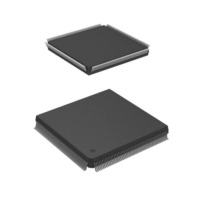
Package
The LFE2-12SE-6QN208I comes in a compact Quad Flat No-Lead (QFN) package.
Essence
The essence of the LFE2-12SE-6QN208I lies in its ability to provide a customizable and efficient solution for digital circuit design and implementation.
Packaging/Quantity
The LFE2-12SE-6QN208I is typically packaged individually and is available in various quantities depending on the manufacturer's specifications.
Specifications
- Model: LFE2-12SE-6QN208I
- Number of Logic Elements: 12,000
- Number of I/O Pins: 208
- Operating Voltage: 1.2V
- Maximum Frequency: 500 MHz
- Package Type: QFN
- Temperature Range: -40°C to +85°C
Detailed Pin Configuration
The LFE2-12SE-6QN208I has a total of 208 I/O pins, which are configurable based on the specific requirements of the application. The pin configuration includes input/output pins, power supply pins, ground pins, and configuration pins.
For a detailed pin configuration diagram, please refer to the datasheet provided by the manufacturer.
Functional Features
- High-performance FPGA with low-power consumption
- Configurable I/O pins for versatile design implementation
- Support for various digital functions and algorithms
- On-chip memory blocks for efficient data storage and retrieval
- Built-in clock management resources for precise timing control
Advantages and Disadvantages
Advantages
- Flexibility in design implementation
- High-performance capabilities
- Low-power consumption
- Reconfigurability for future updates or modifications
- Availability of on-chip resources for enhanced functionality
Disadvantages
- Complexity in programming and configuration
- Higher cost compared to fixed-function integrated circuits
- Limited availability of alternative models with similar specifications
Working Principles
The LFE2-12SE-6QN208I operates based on the principles of field-programmable gate arrays. It consists of a matrix of configurable logic elements interconnected through programmable routing resources. The device can be programmed using hardware description languages (HDL) or graphical tools to implement desired digital functions.
Detailed Application Field Plans
The LFE2-12SE-6QN208I finds applications in various fields, including but not limited to: - Telecommunications - Industrial automation - Automotive electronics - Aerospace and defense - Medical devices - Consumer electronics
In these fields, the LFE2-12SE-6QN208I can be used for tasks such as signal processing, data encryption, image and video processing, control systems, and more.
Detailed and Complete Alternative Models
While the LFE2-12SE-6QN208I offers specific features and specifications, there are alternative models available from different manufacturers that cater to similar requirements. Some notable alternatives include: - Xilinx Spartan-6 FPGA series - Intel Cyclone IV FPGA series - Microsemi SmartFusion2 FPGA series
These alternative models provide a range of options with varying performance, power consumption, and pricing to suit different application needs.
In conclusion, the LFE2-12SE-6QN208I is a high-performance FPGA with low-power consumption, offering flexibility and versatility in digital circuit design. Its configurable I/O pins, on-chip resources, and reprogrammability make it suitable for various applications across different industries. While it has advantages such as flexibility and high performance, it also has disadvantages like complexity in programming and higher cost compared to fixed-function integrated circuits. Alternative models from different manufacturers provide additional options for users seeking similar functionality.
Liệt kê 10 câu hỏi và câu trả lời thường gặp liên quan đến ứng dụng LFE2-12SE-6QN208I trong giải pháp kỹ thuật
Sure! Here are 10 common questions and answers related to the application of LFE2-12SE-6QN208I in technical solutions:
Q: What is the LFE2-12SE-6QN208I? A: The LFE2-12SE-6QN208I is a specific model of Field-Programmable Gate Array (FPGA) manufactured by Lattice Semiconductor.
Q: What are the key features of the LFE2-12SE-6QN208I? A: Some key features of this FPGA include 12,000 Look-Up Tables (LUTs), 6 Input/Output banks, and 208-pin Quad Flat No-Lead (QFN) package.
Q: What are the typical applications of the LFE2-12SE-6QN208I? A: This FPGA is commonly used in various technical solutions such as industrial automation, telecommunications, automotive electronics, and medical devices.
Q: How can I program the LFE2-12SE-6QN208I? A: You can program this FPGA using hardware description languages (HDLs) like VHDL or Verilog, along with appropriate development tools provided by Lattice Semiconductor.
Q: Can I reprogram the LFE2-12SE-6QN208I after it has been programmed once? A: Yes, FPGAs are designed to be reprogrammable, allowing you to modify the functionality of the device as needed.
Q: What voltage levels does the LFE2-12SE-6QN208I support? A: This FPGA supports various voltage levels, including 1.2V core voltage and 3.3V or 2.5V I/O voltage, depending on the specific configuration.
Q: How can I interface the LFE2-12SE-6QN208I with other components or devices? A: The FPGA provides multiple I/O banks that can be configured to support different voltage standards and communication protocols, enabling easy interfacing with other components.
Q: Can the LFE2-12SE-6QN208I handle real-time processing tasks? A: Yes, this FPGA is capable of handling real-time processing tasks due to its high-speed performance and parallel processing capabilities.
Q: Are there any development kits available for the LFE2-12SE-6QN208I? A: Yes, Lattice Semiconductor offers development kits specifically designed for this FPGA, providing a convenient platform for prototyping and testing.
Q: Where can I find technical documentation and support for the LFE2-12SE-6QN208I? A: You can find technical documentation, datasheets, application notes, and support resources on the official website of Lattice Semiconductor or by contacting their customer support team.
Please note that the answers provided here are general and may vary depending on the specific requirements and use cases. It's always recommended to refer to the official documentation and consult with experts for accurate information.