

Xem thông số kỹ thuật để biết chi tiết sản phẩm.
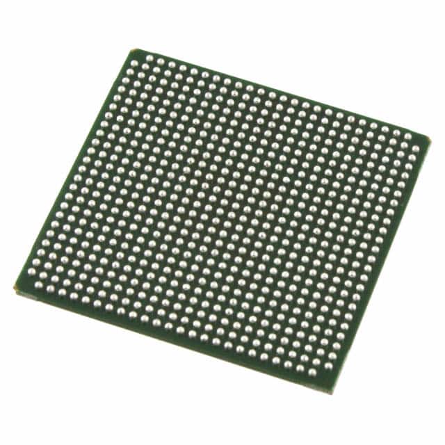
LFE2-35E-6FN672C
Product Overview
Category
LFE2-35E-6FN672C belongs to the category of Field Programmable Gate Arrays (FPGAs).
Use
This product is primarily used in digital logic circuits for various applications such as telecommunications, automotive electronics, consumer electronics, and industrial automation.
Characteristics
- High-performance FPGA with advanced programmability
- Low power consumption
- Flexible and reconfigurable design
- Excellent signal processing capabilities
- Wide range of I/O interfaces
Package
LFE2-35E-6FN672C is available in a compact and durable package suitable for surface mount technology (SMT) assembly.
Essence
The essence of LFE2-35E-6FN672C lies in its ability to provide a customizable and versatile solution for complex digital circuit designs.
Packaging/Quantity
This product is typically packaged in reels or trays, with each reel or tray containing a specific quantity of LFE2-35E-6FN672C units.
Specifications
- Logic Elements: 35,000
- Number of I/O Pins: 672
- Operating Voltage: 1.2V
- Maximum Frequency: 500 MHz
- Embedded Memory: 1,080 Kbits
- Configuration Memory: 4 Mbits
- Package Type: FBGA (Fine-Pitch Ball Grid Array)
- Temperature Range: -40°C to +100°C
Detailed Pin Configuration
The pin configuration of LFE2-35E-6FN672C is as follows:

Functional Features
- High-speed data processing capabilities
- Support for various communication protocols
- On-chip memory resources for efficient data storage
- Built-in security features for protecting sensitive information
- Clock management resources for precise timing control
- Flexible I/O interfaces for seamless integration with external devices
Advantages and Disadvantages
Advantages
- High-performance FPGA suitable for demanding applications
- Low power consumption, reducing overall energy costs
- Reconfigurable design allows for easy updates and modifications
- Wide range of I/O interfaces enable versatile connectivity options
- Excellent signal processing capabilities for complex algorithms
Disadvantages
- Relatively higher cost compared to other programmable logic devices
- Steeper learning curve for beginners due to its complexity
- Limited availability of alternative models in the market
Working Principles
LFE2-35E-6FN672C operates based on the principles of reconfigurable digital logic. It consists of a matrix of configurable logic blocks (CLBs) interconnected through programmable routing resources. The device can be programmed using hardware description languages (HDLs) or graphical tools to implement desired logic functions.
Detailed Application Field Plans
LFE2-35E-6FN672C finds extensive application in various fields, including:
- Telecommunications: Used in base stations, network switches, and routers for high-speed data processing and protocol handling.
- Automotive Electronics: Employed in automotive control systems, infotainment systems, and driver assistance systems for efficient data processing and interface management.
- Consumer Electronics: Integrated into smart TVs, gaming consoles, and multimedia devices to enable advanced functionalities and enhanced user experiences.
- Industrial Automation: Utilized in industrial control systems, robotics, and factory automation equipment for real-time control and monitoring.
Detailed and Complete Alternative Models
While LFE2-35E-6FN672C is a powerful FPGA, there are alternative models available in the market that cater to different requirements. Some notable alternatives include:
- Xilinx Virtex UltraScale+: Offers higher logic capacity and performance for demanding applications.
- Intel Cyclone 10 GX: Provides a cost-effective solution with good performance and power efficiency.
- Microchip PolarFire: Focuses on low-power applications with high-security features.
These alternative models offer varying features and capabilities, allowing designers to choose the most suitable FPGA for their specific needs.
In conclusion, LFE2-35E-6FN672C is a high-performance FPGA that offers flexibility, advanced programmability, and excellent signal processing capabilities. Its wide range of applications and availability of alternative models make it a valuable component in various industries.
Liệt kê 10 câu hỏi và câu trả lời thường gặp liên quan đến ứng dụng LFE2-35E-6FN672C trong giải pháp kỹ thuật
Sure! Here are 10 common questions and answers related to the application of LFE2-35E-6FN672C in technical solutions:
Q: What is the LFE2-35E-6FN672C? A: The LFE2-35E-6FN672C is a specific model of Field-Programmable Gate Array (FPGA) manufactured by Lattice Semiconductor.
Q: What are the key features of the LFE2-35E-6FN672C? A: The key features of this FPGA include 35,000 Look-Up Tables (LUTs), 672 pins, low power consumption, and high-speed performance.
Q: What are some typical applications for the LFE2-35E-6FN672C? A: This FPGA can be used in various applications such as industrial automation, telecommunications, automotive electronics, medical devices, and consumer electronics.
Q: How can I program the LFE2-35E-6FN672C? A: The LFE2-35E-6FN672C can be programmed using hardware description languages (HDL) like VHDL or Verilog, or through graphical programming tools provided by Lattice Semiconductor.
Q: What is the power supply requirement for the LFE2-35E-6FN672C? A: The LFE2-35E-6FN672C typically operates at a voltage range of 1.2V to 3.3V, depending on the specific design requirements.
Q: Can I use the LFE2-35E-6FN672C for real-time signal processing? A: Yes, the LFE2-35E-6FN672C is capable of handling real-time signal processing tasks due to its high-speed performance and programmable nature.
Q: Does the LFE2-35E-6FN672C support external memory interfaces? A: Yes, this FPGA supports various external memory interfaces such as DDR3, DDR4, and LPDDR4, allowing for efficient data storage and retrieval.
Q: Can I use the LFE2-35E-6FN672C in safety-critical applications? A: Yes, the LFE2-35E-6FN672C can be used in safety-critical applications with proper design considerations and adherence to relevant industry standards.
Q: What development tools are available for designing with the LFE2-35E-6FN672C? A: Lattice Semiconductor provides a range of development tools, including the Lattice Diamond software suite, which offers a complete design flow for FPGA development.
Q: Where can I find technical documentation and support for the LFE2-35E-6FN672C? A: Technical documentation, datasheets, application notes, and support resources for the LFE2-35E-6FN672C can be found on the official website of Lattice Semiconductor.