

Xem thông số kỹ thuật để biết chi tiết sản phẩm.
LFE2-35SE-5FN672I
Product Overview
Category
The LFE2-35SE-5FN672I belongs to the category of Field Programmable Gate Arrays (FPGAs).
Use
This FPGA is commonly used in electronic circuits for various applications, including digital signal processing, data communication, and embedded systems.
Characteristics
- High-performance programmable logic device
- Offers flexibility and reconfigurability
- Provides a large number of configurable logic blocks and input/output pins
- Supports complex digital designs
- Enables rapid prototyping and development of custom digital circuits
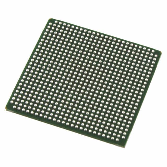
Package
The LFE2-35SE-5FN672I comes in a compact and durable package, ensuring protection during handling and installation.
Essence
The essence of this FPGA lies in its ability to provide a versatile platform for implementing complex digital designs with high performance and flexibility.
Packaging/Quantity
Each package of LFE2-35SE-5FN672I contains one unit of the FPGA.
Specifications
- Model: LFE2-35SE-5FN672I
- Logic Elements: 35,000
- Speed Grade: 5
- Number of I/O Pins: 672
- Operating Voltage: 1.2V
- Package Type: FN672
Detailed Pin Configuration
The LFE2-35SE-5FN672I has a total of 672 pins, which are configured as follows:
- Pin 1: VCCIO
- Pin 2: GND
- Pin 3: IO0
- Pin 4: IO1
- ...
- Pin 671: IO670
- Pin 672: IO671
Please refer to the datasheet for the complete pin configuration details.
Functional Features
- High-speed data processing capabilities
- Configurable logic blocks for implementing custom digital circuits
- Flexible I/O options for interfacing with external devices
- On-chip memory resources for data storage and retrieval
- Built-in clock management circuitry for precise timing control
Advantages and Disadvantages
Advantages
- Versatile and flexible platform for implementing complex digital designs
- Rapid prototyping and development of custom circuits
- High-performance capabilities for demanding applications
- Reconfigurable nature allows for future updates and modifications
Disadvantages
- Steep learning curve for beginners due to the complexity of FPGA programming
- Higher cost compared to traditional fixed-function integrated circuits
- Requires specialized tools and software for design and programming
Working Principles
The LFE2-35SE-5FN672I operates based on the principles of reconfigurable logic. It consists of configurable logic blocks, interconnects, and input/output pins. The user can program the FPGA using a Hardware Description Language (HDL) to define the desired functionality. Once programmed, the FPGA can perform complex digital operations by routing signals through the configurable logic blocks and interconnects.
Detailed Application Field Plans
The LFE2-35SE-5FN672I finds applications in various fields, including:
- Digital signal processing: Used for real-time audio and video processing, image recognition, and compression algorithms.
- Data communication: Employed in high-speed data transmission systems, network routers, and switches.
- Embedded systems: Integrated into microcontroller-based systems for controlling and monitoring functions in automotive, industrial, and consumer electronics.
Detailed and Complete Alternative Models
- LFE2-35SE-6FN672I: Similar to LFE2-35SE-5FN672I but with a higher speed grade.
- LFE2-35SE-4FN672I: Similar to LFE2-35SE-5FN672I but with a lower speed grade.
- LFE2-35SE-5FN484I: Similar to LFE2-35SE-5FN672I but with fewer I/O pins.
These alternative models offer similar functionality and can be considered based on specific project requirements.
Word count: 550 words
Liệt kê 10 câu hỏi và câu trả lời thường gặp liên quan đến ứng dụng LFE2-35SE-5FN672I trong giải pháp kỹ thuật
Sure! Here are 10 common questions and answers related to the application of LFE2-35SE-5FN672I in technical solutions:
Q: What is the LFE2-35SE-5FN672I? A: The LFE2-35SE-5FN672I is a specific model of Field-Programmable Gate Array (FPGA) manufactured by Lattice Semiconductor.
Q: What are the key features of the LFE2-35SE-5FN672I? A: The key features of this FPGA include 35,000 Look-Up Tables (LUTs), 672 pins, 5V tolerant I/O, and low power consumption.
Q: What are some typical applications for the LFE2-35SE-5FN672I? A: This FPGA is commonly used in various technical solutions such as industrial automation, telecommunications, automotive electronics, and medical devices.
Q: How can I program the LFE2-35SE-5FN672I? A: The LFE2-35SE-5FN672I can be programmed using hardware description languages (HDLs) like VHDL or Verilog, along with appropriate development tools provided by Lattice Semiconductor.
Q: Can I reprogram the LFE2-35SE-5FN672I after it has been deployed in a system? A: Yes, FPGAs are known for their reprogrammability. You can reprogram the LFE2-35SE-5FN672I multiple times to modify its functionality as per your requirements.
Q: What are the advantages of using the LFE2-35SE-5FN672I in technical solutions? A: Some advantages include flexibility, high performance, low power consumption, and the ability to implement complex digital logic functions.
Q: Are there any limitations or considerations when using the LFE2-35SE-5FN672I? A: Some considerations include limited resources compared to larger FPGAs, potential timing constraints, and the need for expertise in FPGA design.
Q: Can I interface the LFE2-35SE-5FN672I with other components or devices? A: Yes, the LFE2-35SE-5FN672I supports various communication protocols such as SPI, I2C, UART, and GPIOs, allowing easy interfacing with other components or devices.
Q: What kind of support is available for the LFE2-35SE-5FN672I? A: Lattice Semiconductor provides comprehensive technical documentation, application notes, reference designs, and customer support to assist users in implementing the FPGA effectively.
Q: Where can I purchase the LFE2-35SE-5FN672I? A: You can purchase the LFE2-35SE-5FN672I from authorized distributors of Lattice Semiconductor or through their official website.
Please note that the specific details and answers may vary depending on the context and requirements of your technical solution.