

Xem thông số kỹ thuật để biết chi tiết sản phẩm.
LFE2-35SE-6FN672I
Product Overview
Category
The LFE2-35SE-6FN672I belongs to the category of Field Programmable Gate Arrays (FPGAs).
Use
FPGAs are integrated circuits that can be programmed and reprogrammed to perform various digital functions. The LFE2-35SE-6FN672I is specifically designed for applications requiring high-performance and low-power consumption.
Characteristics
- High performance: The LFE2-35SE-6FN672I offers a combination of speed and flexibility, making it suitable for demanding applications.
- Low power consumption: This FPGA is designed to minimize power usage, making it energy-efficient.
- Programmability: The LFE2-35SE-6FN672I can be easily programmed and reconfigured to adapt to different requirements.
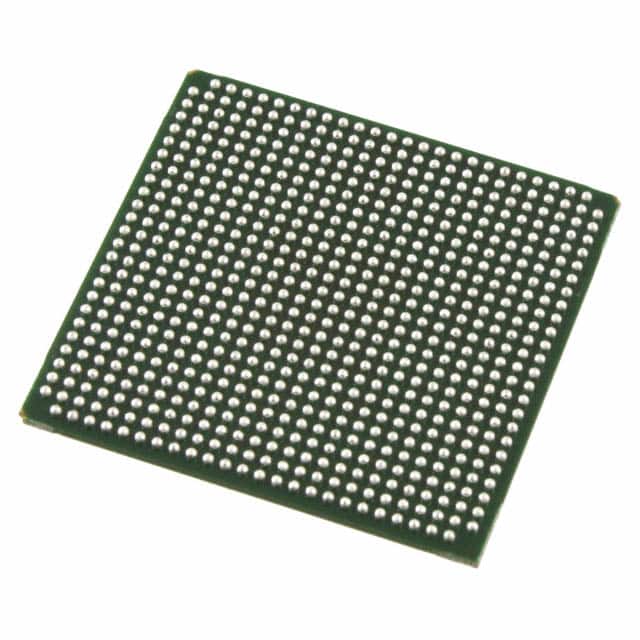
- Compact package: It comes in a 672-pin FineLine BGA package, ensuring efficient use of space on circuit boards.
- Versatility: The LFE2-35SE-6FN672I supports a wide range of applications due to its flexible architecture.
Packaging/Quantity
The LFE2-35SE-6FN672I is typically packaged individually and is available in various quantities depending on the customer's needs.
Specifications
- Device family: LatticeECP2M™
- Logic elements: 33,216
- Embedded memory: 1,152 Kbits
- Maximum user I/Os: 622
- Operating voltage: 1.2V
- Speed grade: -6
- Package type: FineLine BGA
- Package pins: 672
Detailed Pin Configuration
The LFE2-35SE-6FN672I has a total of 672 pins, each serving a specific purpose. A detailed pin configuration diagram can be found in the product datasheet.
Functional Features
- High-speed performance: The LFE2-35SE-6FN672I offers fast data processing capabilities, making it suitable for applications requiring real-time operations.
- Flexible I/O options: It provides a large number of user I/Os, allowing for versatile connectivity with other components.
- On-chip memory: The embedded memory enables efficient data storage and retrieval, reducing the need for external memory devices.
- Low power consumption: The FPGA is designed to minimize power usage, making it ideal for battery-powered or energy-efficient applications.
- Configurable logic blocks: The LFE2-35SE-6FN672I contains programmable logic blocks that can be customized to implement various digital functions.
Advantages and Disadvantages
Advantages
- High-performance capabilities
- Low power consumption
- Versatile and flexible architecture
- Compact package size
- Easy programmability and reconfigurability
Disadvantages
- Limited availability of alternative models
- Higher cost compared to some other FPGA options
Working Principles
The LFE2-35SE-6FN672I operates based on the principles of field-programmable gate arrays. It consists of configurable logic blocks interconnected through programmable routing resources. These logic blocks can be programmed using hardware description languages to implement desired digital functions. The FPGA's internal configuration memory stores the programming information, allowing for reconfiguration as needed.
Detailed Application Field Plans
The LFE2-35SE-6FN672I finds applications in various fields, including: 1. Telecommunications: It can be used in network routers, switches, and communication equipment for high-speed data processing. 2. Industrial automation: The FPGA's flexibility makes it suitable for controlling and monitoring complex industrial processes. 3. Medical devices: It can be utilized in medical imaging systems, patient monitoring devices, and diagnostic equipment. 4. Aerospace and defense: The LFE2-35SE-6FN672I can be employed in radar systems, avionics, and military communication devices. 5. Automotive electronics: It finds applications in advanced driver-assistance systems (ADAS), infotainment systems, and engine control units.
Detailed and Complete Alternative Models
While the LFE2-35SE-6FN672I offers unique features, there are alternative FPGA models available from different manufacturers that serve similar purposes. Some notable alternatives include: - Xilinx Spartan-6 XC6SLX25 - Intel Cyclone IV EP4CE22 - Microsemi SmartFusion2 M2S010
These alternatives provide a range of options with varying specifications and capabilities, allowing designers to choose the most suitable FPGA for their specific requirements.
In conclusion, the LFE2-35SE-6FN672I is a high-performance and low-power FPGA that offers versatility and flexibility for various applications. Its compact package, programmability, and functional features make it an attractive choice for designers seeking efficient digital solutions.
Liệt kê 10 câu hỏi và câu trả lời thường gặp liên quan đến ứng dụng LFE2-35SE-6FN672I trong giải pháp kỹ thuật
Sure! Here are 10 common questions and answers related to the application of LFE2-35SE-6FN672I in technical solutions:
Q: What is the LFE2-35SE-6FN672I? A: The LFE2-35SE-6FN672I is a specific model of Field-Programmable Gate Array (FPGA) manufactured by Lattice Semiconductor.
Q: What are the key features of the LFE2-35SE-6FN672I? A: The key features of this FPGA include 35,000 Look-Up Tables (LUTs), 672 pins, 6-input function capability, and support for various I/O standards.
Q: In what technical solutions can the LFE2-35SE-6FN672I be used? A: This FPGA can be used in a wide range of applications such as industrial automation, telecommunications, automotive electronics, medical devices, and more.
Q: How can the LFE2-35SE-6FN672I be programmed? A: The LFE2-35SE-6FN672I can be programmed using Hardware Description Languages (HDLs) like VHDL or Verilog, or through graphical programming tools provided by Lattice Semiconductor.
Q: What are the advantages of using the LFE2-35SE-6FN672I in technical solutions? A: Some advantages include its flexibility, reprogrammability, low power consumption, high performance, and ability to integrate multiple functions into a single chip.
Q: Can the LFE2-35SE-6FN672I interface with other components or devices? A: Yes, the LFE2-35SE-6FN672I supports various communication protocols and can interface with other components or devices through its I/O pins.
Q: What is the maximum operating frequency of the LFE2-35SE-6FN672I? A: The maximum operating frequency of this FPGA depends on the specific design and implementation, but it can typically reach several hundred megahertz (MHz) or even gigahertz (GHz).
Q: Are there any development tools available for designing with the LFE2-35SE-6FN672I? A: Yes, Lattice Semiconductor provides development tools like Lattice Diamond or Lattice Radiant software suites that assist in designing, simulating, and programming the FPGA.
Q: Can the LFE2-35SE-6FN672I be used in safety-critical applications? A: Yes, the LFE2-35SE-6FN672I can be used in safety-critical applications as long as proper design practices and safety measures are followed to ensure reliability and fault tolerance.
Q: Where can I find more information about the LFE2-35SE-6FN672I and its application in technical solutions? A: You can find more detailed information, datasheets, reference designs, and application notes on the official website of Lattice Semiconductor or by contacting their technical support team.