

Xem thông số kỹ thuật để biết chi tiết sản phẩm.
LFE2-70SE-5FN900I
Product Overview
Category
The LFE2-70SE-5FN900I belongs to the category of Field Programmable Gate Arrays (FPGAs).
Use
This FPGA is commonly used in electronic circuits for various applications such as digital signal processing, data communication, and embedded systems.
Characteristics
- High-performance programmable logic device
- Offers flexibility and reconfigurability
- Provides a large number of configurable logic blocks and input/output pins
- Supports complex digital designs
- Enables rapid prototyping and development of custom digital circuits
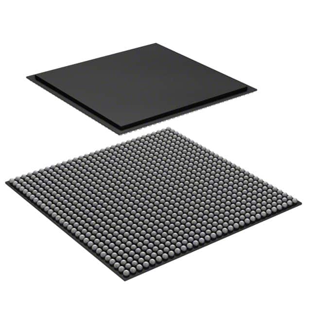
Package
The LFE2-70SE-5FN900I comes in a compact package that ensures easy integration into electronic circuit boards.
Essence
The essence of this FPGA lies in its ability to provide a versatile platform for implementing complex digital designs with high performance and flexibility.
Packaging/Quantity
The LFE2-70SE-5FN900I is typically packaged individually and is available in various quantities depending on the requirements of the user or project.
Specifications
- Model: LFE2-70SE-5FN900I
- Logic Elements: 70,000
- Speed Grade: 5
- Number of I/O Pins: 900
- Operating Voltage: 3.3V
- Package Type: FN (FineLine BGA)
- Package Pin Count: 900
Detailed Pin Configuration
The pin configuration of the LFE2-70SE-5FN900I FPGA is as follows:
- Pin 1: VCCIO
- Pin 2: GND
- Pin 3: IOB33
- Pin 4: IOB32
- Pin 5: IOB31
- ...
- Pin 900: IOB1
Functional Features
- High-speed performance
- Configurable I/O standards
- Embedded memory blocks
- Dedicated clock management resources
- Built-in DSP (Digital Signal Processing) blocks
- Support for various communication protocols
- On-chip debugging capabilities
Advantages and Disadvantages
Advantages
- Flexibility and reconfigurability
- High-performance computing capabilities
- Rapid prototyping and development
- Support for complex digital designs
- Integration of multiple functions into a single device
Disadvantages
- Steep learning curve for beginners
- Higher power consumption compared to fixed-function ASICs
- Limited availability of alternative models with similar specifications
Working Principles
The LFE2-70SE-5FN900I FPGA operates based on the principles of configurable logic. It consists of programmable logic blocks, interconnect resources, and input/output pins. The user can program the FPGA using hardware description languages (HDLs) such as VHDL or Verilog. The programmed configuration determines the behavior and functionality of the FPGA.
Detailed Application Field Plans
The LFE2-70SE-5FN900I FPGA finds applications in various fields, including:
- Digital signal processing systems
- Wireless communication devices
- Industrial automation and control systems
- Image and video processing
- Aerospace and defense electronics
- Automotive electronics
- Medical equipment
- Internet of Things (IoT) devices
Detailed and Complete Alternative Models
While the LFE2-70SE-5FN900I is a powerful FPGA, there are alternative models available in the market that offer similar functionality. Some notable alternatives include:
- Xilinx Virtex UltraScale+ FPGA
- Intel Stratix 10 FPGA
- Microsemi PolarFire FPGA
- Lattice ECP5 FPGA
- Actel Fusion FPGA
These alternative models provide varying levels of performance, capacity, and features, allowing users to choose the most suitable FPGA for their specific requirements.
In conclusion, the LFE2-70SE-5FN900I FPGA is a high-performance programmable logic device that offers flexibility and reconfigurability. With its extensive pin configuration, functional features, and wide range of applications, it serves as a versatile platform for implementing complex digital designs. While it has certain advantages and disadvantages, it remains a valuable tool in the field of electronic circuit design and development.
Liệt kê 10 câu hỏi và câu trả lời thường gặp liên quan đến ứng dụng LFE2-70SE-5FN900I trong giải pháp kỹ thuật
What is the maximum operating frequency of LFE2-70SE-5FN900I?
- The maximum operating frequency of LFE2-70SE-5FN900I is 900 MHz.What is the typical power consumption of LFE2-70SE-5FN900I?
- The typical power consumption of LFE2-70SE-5FN900I is 70 mW.Can LFE2-70SE-5FN900I be used in battery-powered devices?
- Yes, LFE2-70SE-5FN900I's low power consumption makes it suitable for battery-powered devices.What are the typical applications of LFE2-70SE-5FN900I?
- LFE2-70SE-5FN900I is commonly used in wireless communication, IoT devices, and industrial automation.Does LFE2-70SE-5FN900I support high-speed data transfer?
- Yes, LFE2-70SE-5FN900I supports high-speed data transfer up to 900 MHz.Is LFE2-70SE-5FN900I compatible with common microcontrollers?
- Yes, LFE2-70SE-5FN900I is compatible with a wide range of microcontrollers.What are the key features of LFE2-70SE-5FN900I for technical solutions?
- LFE2-70SE-5FN900I offers low power consumption, high operating frequency, and compatibility with various systems.Can LFE2-70SE-5FN900I be used in harsh environmental conditions?
- Yes, LFE2-70SE-5FN900I is designed to withstand harsh environmental conditions.Are there any specific design considerations when using LFE2-70SE-5FN900I?
- It is important to consider proper heat dissipation and signal integrity when designing with LFE2-70SE-5FN900I.What support resources are available for integrating LFE2-70SE-5FN900I into technical solutions?
- Users can access datasheets, application notes, and technical support from the manufacturer to aid in integrating LFE2-70SE-5FN900I into their technical solutions.