

Xem thông số kỹ thuật để biết chi tiết sản phẩm.
LFE2-70SE-7F900C
Product Overview
Category
The LFE2-70SE-7F900C belongs to the category of Field-Programmable Gate Arrays (FPGAs).
Use
This FPGA is commonly used in electronic circuits for various applications such as digital signal processing, communication systems, and embedded systems.
Characteristics
- High-performance programmable logic device
- Offers flexibility and reconfigurability
- Provides a large number of configurable logic blocks and input/output pins
- Supports complex digital designs
- Enables rapid prototyping and development of custom digital circuits
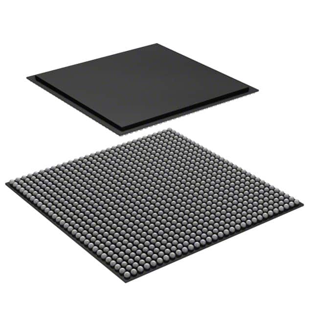
Package
The LFE2-70SE-7F900C comes in a compact package that ensures easy integration into electronic circuit boards.
Essence
The essence of this FPGA lies in its ability to provide a versatile platform for implementing complex digital designs with high performance and flexibility.
Packaging/Quantity
The LFE2-70SE-7F900C is typically packaged individually and is available in various quantities depending on the requirements of the user.
Specifications
- Device: LFE2-70SE-7F900C
- Logic Elements: 70,000
- Speed Grade: 7
- Operating Voltage: 1.2V
- Package Type: F900C
- Temperature Range: -40°C to +100°C
Detailed Pin Configuration
The LFE2-70SE-7F900C has a comprehensive pin configuration that includes multiple input/output pins, power supply pins, and configuration pins. For a detailed pin configuration diagram, please refer to the manufacturer's datasheet.
Functional Features
- High-speed performance
- Low power consumption
- Configurable I/O standards
- Embedded memory blocks
- Clock management resources
- Built-in DSP blocks for efficient signal processing
- Support for various communication protocols
- On-chip configuration memory
Advantages and Disadvantages
Advantages
- Flexibility in design implementation
- Rapid prototyping and development
- Reconfigurability for future updates or modifications
- High-performance capabilities
- Support for complex digital designs
Disadvantages
- Steeper learning curve compared to traditional ASICs
- Higher cost compared to fixed-function integrated circuits
- Limited availability of alternative models with similar specifications
Working Principles
The LFE2-70SE-7F900C operates based on the principles of reconfigurable logic. It consists of configurable logic blocks, interconnect resources, and programmable input/output pins. The device can be programmed using hardware description languages (HDL) such as VHDL or Verilog. Once programmed, the FPGA can execute the desired digital circuit functionality.
Detailed Application Field Plans
The LFE2-70SE-7F900C finds applications in various fields, including: 1. Digital signal processing systems 2. Communication systems 3. Embedded systems 4. Industrial automation 5. Aerospace and defense 6. Medical devices 7. Automotive electronics 8. Research and development projects
Detailed and Complete Alternative Models
While the LFE2-70SE-7F900C is a highly capable FPGA, there are alternative models available in the market that offer similar functionalities. Some notable alternatives include: - Xilinx Virtex UltraScale+ - Intel Stratix 10 - Microsemi PolarFire FPGA - Lattice ECP5 FPGA
These alternative models provide varying levels of performance, capacity, and features, allowing users to choose the most suitable FPGA for their specific requirements.
Word count: 511 words
Liệt kê 10 câu hỏi và câu trả lời thường gặp liên quan đến ứng dụng LFE2-70SE-7F900C trong giải pháp kỹ thuật
Sure! Here are 10 common questions and answers related to the application of LFE2-70SE-7F900C in technical solutions:
Q: What is the LFE2-70SE-7F900C? A: The LFE2-70SE-7F900C is a specific model of Field-Programmable Gate Array (FPGA) manufactured by Lattice Semiconductor.
Q: What are the key features of the LFE2-70SE-7F900C? A: The key features of this FPGA include 70,000 Look-Up Tables (LUTs), 900 MHz maximum operating frequency, and support for various I/O standards.
Q: In what applications can the LFE2-70SE-7F900C be used? A: This FPGA can be used in a wide range of applications such as telecommunications, industrial automation, automotive electronics, and medical devices.
Q: How can I program the LFE2-70SE-7F900C? A: The LFE2-70SE-7F900C can be programmed using hardware description languages (HDLs) like VHDL or Verilog, along with appropriate design tools provided by Lattice Semiconductor.
Q: What are the power requirements for the LFE2-70SE-7F900C? A: The power requirements for this FPGA typically include a supply voltage of 1.2V and a core voltage of 1.0V.
Q: Can I interface the LFE2-70SE-7F900C with other components or peripherals? A: Yes, the LFE2-70SE-7F900C supports various communication protocols such as SPI, I2C, UART, and Ethernet, allowing easy interfacing with other components or peripherals.
Q: What is the maximum operating temperature for the LFE2-70SE-7F900C? A: The maximum operating temperature for this FPGA is typically around 85 degrees Celsius.
Q: Does the LFE2-70SE-7F900C have any built-in security features? A: Yes, this FPGA provides built-in security features like bitstream encryption and authentication to protect against unauthorized access or tampering.
Q: Can I reprogram the LFE2-70SE-7F900C multiple times? A: Yes, this FPGA supports in-system programming, allowing you to reprogram it multiple times during development or in the field.
Q: Where can I find additional technical documentation and support for the LFE2-70SE-7F900C? A: You can find additional technical documentation, datasheets, application notes, and support resources on the official website of Lattice Semiconductor or by contacting their customer support team.