

Xem thông số kỹ thuật để biết chi tiết sản phẩm.
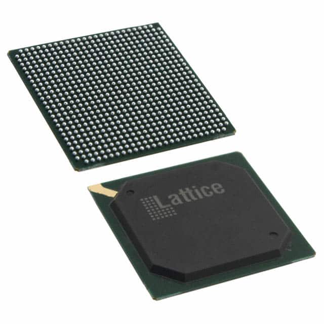
LFE2M50E-6FN672C
Product Overview
Category
The LFE2M50E-6FN672C belongs to the category of Field Programmable Gate Arrays (FPGAs).
Use
FPGAs are integrated circuits that can be programmed and reprogrammed to perform various digital functions. The LFE2M50E-6FN672C is specifically designed for applications requiring high-performance and low-power consumption.
Characteristics
- High performance: The LFE2M50E-6FN672C offers a large number of logic elements and advanced features, enabling complex digital designs.
- Low power consumption: This FPGA incorporates power-saving techniques, making it suitable for battery-powered devices or energy-efficient systems.
- Flexible configuration: The LFE2M50E-6FN672C allows users to customize the circuitry according to their specific requirements, providing design flexibility.
- Reliable operation: With built-in error detection and correction mechanisms, this FPGA ensures reliable and error-free operation.
Package and Quantity
The LFE2M50E-6FN672C is available in a 672-ball FineLine BGA package. It is typically sold individually.
Specifications
- Logic Elements: 50,000
- Embedded Memory: 1,728 Kbits
- Maximum User I/Os: 381
- Clock Management Tiles: 4
- DSP Blocks: 120
- Maximum Internal Frequency: 400 MHz
- Operating Voltage: 1.2V
- Package Dimensions: 23mm x 23mm
Detailed Pin Configuration
The LFE2M50E-6FN672C has a total of 672 pins, each serving a specific purpose within the FPGA's architecture. A detailed pin configuration diagram can be found in the product datasheet.
Functional Features
- High-speed data processing: The LFE2M50E-6FN672C offers fast data processing capabilities, making it suitable for applications requiring real-time performance.
- Flexible I/O interfaces: This FPGA supports various communication protocols, including UART, SPI, I2C, and Ethernet, enabling seamless integration with external devices.
- On-chip memory: The embedded memory blocks allow for efficient storage and retrieval of data, reducing the need for external memory components.
- Configurable logic: The LFE2M50E-6FN672C allows users to implement complex digital functions by configuring the logic elements according to their specific requirements.
Advantages and Disadvantages
Advantages
- High-performance capabilities
- Low power consumption
- Design flexibility
- Reliable operation
- Support for various communication protocols
Disadvantages
- Limited number of user I/Os compared to larger FPGAs
- Higher cost compared to simpler programmable logic devices
Working Principles
The LFE2M50E-6FN672C operates based on the principles of reconfigurable computing. It consists of a matrix of configurable logic elements interconnected through programmable routing resources. These logic elements can be programmed to perform specific digital functions, allowing for the implementation of complex circuits within a single integrated circuit.
Detailed Application Field Plans
The LFE2M50E-6FN672C finds applications in various fields, including:
- Communications: Used in wireless base stations, routers, and network switches to handle high-speed data processing and protocol conversion.
- Industrial Automation: Employed in control systems, robotics, and machine vision applications to enable real-time data processing and precise control.
- Automotive: Integrated into advanced driver assistance systems (ADAS) and infotainment systems to support image processing, sensor fusion, and connectivity features.
- Aerospace and Defense: Utilized in radar systems, avionics, and secure communication systems to handle complex signal processing and encryption algorithms.
Detailed and Complete Alternative Models
- LFE2M50E-6FN672C-5I: Similar to the LFE2M50E-6FN672C, but operates at a maximum internal frequency of 500 MHz.
- LFE2M50E-6FN672C-8I: Offers increased logic capacity compared to the LFE2M50E-6FN672C, with 80,000 logic elements.
These alternative models provide options for users with specific performance or capacity requirements.
In conclusion, the LFE2M50E-6FN672C is a high-performance FPGA that combines flexibility, low power consumption, and reliability. Its advanced features make it suitable for a wide range of applications in various industries.
Liệt kê 10 câu hỏi và câu trả lời thường gặp liên quan đến ứng dụng LFE2M50E-6FN672C trong giải pháp kỹ thuật
Sure! Here are 10 common questions and answers related to the application of LFE2M50E-6FN672C in technical solutions:
Q: What is the LFE2M50E-6FN672C? A: The LFE2M50E-6FN672C is a specific model of Field-Programmable Gate Array (FPGA) manufactured by Lattice Semiconductor.
Q: What are the key features of the LFE2M50E-6FN672C? A: The key features of this FPGA include 50,000 Look-Up Tables (LUTs), 672-pin Fine-Pitch Ball Grid Array (FBGA) package, and support for various I/O standards.
Q: What are the typical applications of the LFE2M50E-6FN672C? A: This FPGA is commonly used in applications such as industrial automation, telecommunications, automotive electronics, and high-performance computing.
Q: How can I program the LFE2M50E-6FN672C? A: You can program this FPGA using the Lattice Diamond design software, which provides a graphical interface for designing and programming the device.
Q: What voltage levels does the LFE2M50E-6FN672C support? A: This FPGA supports various voltage levels, including 1.2V core voltage and 3.3V or 2.5V I/O voltage, depending on the configuration.
Q: Can I use the LFE2M50E-6FN672C in a low-power application? A: Yes, this FPGA offers power-saving features such as dynamic power management and multiple power supply options, making it suitable for low-power designs.
Q: Does the LFE2M50E-6FN672C support high-speed interfaces? A: Yes, this FPGA supports various high-speed interfaces like DDR3/DDR4 memory interfaces, PCIe, Ethernet, and USB, enabling connectivity with other devices.
Q: Can I use the LFE2M50E-6FN672C for real-time signal processing? A: Absolutely! This FPGA provides dedicated DSP blocks, which are optimized for performing complex mathematical operations required in real-time signal processing applications.
Q: What development tools are available for designing with the LFE2M50E-6FN672C? A: Lattice Semiconductor provides a comprehensive suite of development tools, including the Lattice Diamond design software, IP cores, reference designs, and application notes.
Q: Where can I find technical documentation and support for the LFE2M50E-6FN672C? A: You can find technical documentation, datasheets, user guides, and support resources on the official website of Lattice Semiconductor or by contacting their customer support team.
Please note that the answers provided here are general and may vary depending on specific requirements and use cases. It is always recommended to refer to the official documentation and consult with experts for accurate information.