

Xem thông số kỹ thuật để biết chi tiết sản phẩm.
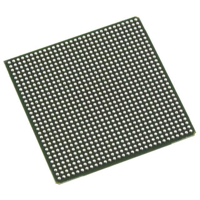
LFE2M50SE-5FN900I
Product Overview
Category
The LFE2M50SE-5FN900I belongs to the category of Field Programmable Gate Arrays (FPGAs).
Use
This FPGA is commonly used in various electronic applications that require high-performance digital logic circuits. It provides a flexible and customizable solution for implementing complex digital designs.
Characteristics
- High-density programmable logic device
- Low power consumption
- High-speed performance
- Large number of configurable I/O pins
- Built-in memory blocks and DSP slices
- Support for various communication protocols
Package
The LFE2M50SE-5FN900I is available in a compact and durable package, ensuring easy integration into electronic systems. The package type may vary depending on the manufacturer.
Essence
The essence of the LFE2M50SE-5FN900I lies in its ability to provide a reconfigurable hardware platform that allows users to implement custom digital designs without the need for dedicated application-specific integrated circuits (ASICs).
Packaging/Quantity
The LFE2M50SE-5FN900I is typically sold individually or in small quantities, depending on the supplier's packaging options.
Specifications
- Logic Elements: 50,000
- Embedded Memory: Up to 4,608 Kbits
- DSP Slices: Up to 360
- I/O Pins: Up to 900
- Operating Voltage: 1.2V
- Maximum Frequency: 500 MHz
- Configuration Memory: Flash-based
Detailed Pin Configuration
The LFE2M50SE-5FN900I has a comprehensive pin configuration, allowing for versatile connectivity and integration within electronic systems. For detailed pin assignments, please refer to the manufacturer's datasheet.
Functional Features
- Reconfigurable logic elements for implementing complex digital circuits
- Embedded memory blocks for efficient data storage and retrieval
- DSP slices for performing high-speed digital signal processing operations
- Flexible I/O pins for interfacing with external devices
- Support for various communication protocols, such as UART, SPI, and I2C
- On-chip clock management resources for precise timing control
Advantages and Disadvantages
Advantages
- Flexibility: Allows for the implementation of custom digital designs without the need for ASICs.
- Cost-effective: Reduces the development cost compared to designing dedicated integrated circuits.
- Time-to-market: Enables faster prototyping and product development cycles.
- High-performance: Offers high-speed operation and efficient resource utilization.
Disadvantages
- Learning curve: Requires knowledge of hardware description languages (HDL) and FPGA design methodologies.
- Limited scalability: The number of logic elements and resources may be insufficient for extremely complex designs.
- Power consumption: FPGAs generally consume more power compared to application-specific integrated circuits.
Working Principles
The LFE2M50SE-5FN900I operates based on the principles of reconfigurable computing. It consists of an array of programmable logic elements interconnected through configurable routing resources. These logic elements can be programmed to implement desired digital functions using hardware description languages. The configuration data is stored in the flash-based memory and loaded during startup.
Detailed Application Field Plans
The LFE2M50SE-5FN900I finds applications in various fields, including: 1. Telecommunications: Used in base stations, network routers, and communication equipment for signal processing and protocol handling. 2. Industrial Automation: Employed in control systems, robotics, and machine vision applications for real-time data processing and control. 3. Aerospace and Defense: Utilized in radar systems, avionics, and military-grade electronics for high-performance signal processing and encryption. 4. Medical Devices: Integrated into medical imaging systems, patient monitoring devices, and diagnostic equipment for data acquisition and processing. 5. Automotive: Incorporated in advanced driver-assistance systems (ADAS), infotainment systems, and engine control units for enhanced functionality.
Detailed and Complete Alternative Models
- LFE2M50SE-6FN900I: Similar to the LFE2M50SE-5FN900I but with a higher maximum frequency of 600 MHz.
- LFE2M50SE-4FN900I: A lower-cost variant with reduced logic elements and I/O pins but suitable for less complex designs.
- LFE2M50SE-5FN484C: Offers the same logic capacity but in a different package and pin configuration.
These alternative models provide options based on specific project requirements, budget constraints, and desired performance levels.
In conclusion, the LFE2M50SE-5FN900I is a high-density FPGA that offers flexibility, high-performance, and a wide range of applications. Its reconfigurable nature makes it an ideal choice for various electronic design projects.
Liệt kê 10 câu hỏi và câu trả lời thường gặp liên quan đến ứng dụng LFE2M50SE-5FN900I trong giải pháp kỹ thuật
Sure! Here are 10 common questions and answers related to the application of LFE2M50SE-5FN900I in technical solutions:
Q: What is the LFE2M50SE-5FN900I? A: The LFE2M50SE-5FN900I is a specific model of Field-Programmable Gate Array (FPGA) manufactured by Lattice Semiconductor.
Q: What are the key features of the LFE2M50SE-5FN900I? A: Some key features include 50,000 Look-Up Tables (LUTs), 900 Input/Output (I/O) pins, and support for various communication protocols like PCIe, Ethernet, and USB.
Q: What are the typical applications of the LFE2M50SE-5FN900I? A: The LFE2M50SE-5FN900I is commonly used in applications such as industrial automation, telecommunications, automotive electronics, and medical devices.
Q: How can I program the LFE2M50SE-5FN900I? A: The LFE2M50SE-5FN900I can be programmed using hardware description languages (HDL) like VHDL or Verilog, which are then synthesized and implemented using design software provided by Lattice Semiconductor.
Q: Can the LFE2M50SE-5FN900I be reprogrammed after deployment? A: Yes, the LFE2M50SE-5FN900I is a reprogrammable FPGA, allowing for updates and modifications to the design even after it has been deployed.
Q: What are the power requirements for the LFE2M50SE-5FN900I? A: The LFE2M50SE-5FN900I typically operates at a voltage range of 1.2V to 3.3V, with power consumption varying based on the design and utilization.
Q: Can the LFE2M50SE-5FN900I interface with other components or microcontrollers? A: Yes, the LFE2M50SE-5FN900I can interface with other components or microcontrollers through its numerous I/O pins, allowing for seamless integration into larger systems.
Q: Are there any development boards available for the LFE2M50SE-5FN900I? A: Yes, Lattice Semiconductor provides development boards specifically designed for the LFE2M50SE-5FN900I, which include necessary connectors and peripherals for prototyping and testing.
Q: What kind of support is available for the LFE2M50SE-5FN900I? A: Lattice Semiconductor offers technical documentation, application notes, reference designs, and online forums to provide support for users working with the LFE2M50SE-5FN900I.
Q: Where can I purchase the LFE2M50SE-5FN900I? A: The LFE2M50SE-5FN900I can be purchased from authorized distributors of Lattice Semiconductor products or directly from their website.