

Xem thông số kỹ thuật để biết chi tiết sản phẩm.
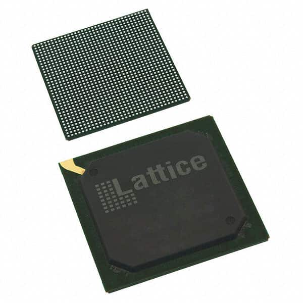
LFE3-150EA-8FN1156C
Product Overview
Category
The LFE3-150EA-8FN1156C belongs to the category of Field Programmable Gate Arrays (FPGAs).
Use
This FPGA is commonly used in electronic systems for various applications such as digital signal processing, communication systems, and high-performance computing.
Characteristics
- High-speed performance
- Reconfigurable logic
- Low power consumption
- Large capacity
- Flexible design options
Package
The LFE3-150EA-8FN1156C comes in a compact package that ensures easy integration into electronic systems. It is designed to be mounted on a printed circuit board (PCB) using surface mount technology (SMT).
Essence
The essence of the LFE3-150EA-8FN1156C lies in its ability to provide a customizable hardware platform that allows users to implement complex digital designs efficiently.
Packaging/Quantity
The LFE3-150EA-8FN1156C is typically packaged in trays or reels, depending on the manufacturer's specifications. The quantity per package may vary, but it is commonly available in quantities suitable for both prototyping and production purposes.
Specifications
- FPGA Family: LatticeECP3
- Logic Elements: 149,760
- Embedded Memory: Up to 4.9 Mb
- DSP Slices: 360
- Maximum User I/Os: 1,156
- Operating Voltage: 1.2V
- Package Type: FBGA
- Package Pins: 1156
- Temperature Range: -40°C to +100°C
Detailed Pin Configuration
The LFE3-150EA-8FN1156C has a total of 1156 pins, each serving a specific purpose in the FPGA's functionality. For detailed pin configuration, please refer to the manufacturer's datasheet or user manual.
Functional Features
- High-speed serial transceivers
- Flexible I/O standards support
- Embedded memory blocks
- Clock management resources
- Programmable routing architecture
- On-chip debugging capabilities
Advantages and Disadvantages
Advantages
- Versatile and customizable design options
- High-performance computing capabilities
- Low power consumption
- Reconfigurable for future updates or modifications
- Suitable for a wide range of applications
Disadvantages
- Steep learning curve for beginners
- Requires specialized knowledge for optimal utilization
- Higher cost compared to other programmable logic devices
Working Principles
The LFE3-150EA-8FN1156C operates based on the principles of reconfigurable logic. It consists of an array of configurable logic elements interconnected through programmable routing resources. These logic elements can be programmed to implement various digital functions, allowing users to create custom designs tailored to their specific requirements.
Detailed Application Field Plans
The LFE3-150EA-8FN1156C finds extensive use in the following application fields:
Digital Signal Processing (DSP) Systems: The FPGA's high-speed performance and embedded memory make it ideal for implementing complex DSP algorithms used in audio and video processing, telecommunications, and radar systems.
Communication Systems: With its flexible I/O standards support and high-speed serial transceivers, the FPGA is well-suited for designing communication systems such as Ethernet switches, wireless base stations, and network routers.
High-Performance Computing: The LFE3-150EA-8FN1156C's large capacity and programmable routing architecture enable the implementation of high-performance computing systems, including data centers, scientific simulations, and image processing.
Industrial Automation: The FPGA's reconfigurable nature makes it suitable for industrial automation applications, such as motor control, robotics, and process monitoring.
Detailed and Complete Alternative Models
Xilinx Virtex-7 XC7VX690T: This FPGA offers similar high-performance computing capabilities with a larger logic capacity.
Intel Cyclone V GX: With its low power consumption and cost-effective design, this FPGA is an alternative for applications with lower performance requirements.
Microsemi SmartFusion2 M2S010: This FPGA combines programmable logic with a microcontroller subsystem, making it suitable for embedded system designs.
Altera MAX 10M08SAE144C8G: This low-cost FPGA provides a balance between performance and affordability, making it suitable for small-scale projects.
These alternative models offer different features and price points, allowing users to choose the most appropriate FPGA for their specific needs.
In conclusion, the LFE3-150EA-8FN1156C is a versatile and high-performance FPGA that finds application in various fields, including digital signal processing, communication systems, high-performance computing, and industrial automation. Its reconfigurable nature, large capacity, and flexible design options make it a
Liệt kê 10 câu hỏi và câu trả lời thường gặp liên quan đến ứng dụng LFE3-150EA-8FN1156C trong giải pháp kỹ thuật
Sure! Here are 10 common questions and answers related to the application of LFE3-150EA-8FN1156C in technical solutions:
Q: What is the LFE3-150EA-8FN1156C? A: The LFE3-150EA-8FN1156C is a field-programmable gate array (FPGA) manufactured by Lattice Semiconductor.
Q: What are the key features of the LFE3-150EA-8FN1156C? A: The key features of this FPGA include 150,000 logic elements, 8 high-speed SERDES channels, and support for various I/O standards.
Q: What are some typical applications of the LFE3-150EA-8FN1156C? A: This FPGA is commonly used in applications such as telecommunications, networking, industrial automation, video processing, and high-performance computing.
Q: How can I program the LFE3-150EA-8FN1156C? A: You can program this FPGA using Lattice Diamond design software or other compatible programming tools provided by Lattice Semiconductor.
Q: What is the power supply requirement for the LFE3-150EA-8FN1156C? A: The recommended power supply voltage for this FPGA is typically 1.2V, but it also supports a range of voltages from 0.9V to 1.35V.
Q: Can I interface the LFE3-150EA-8FN1156C with external devices? A: Yes, this FPGA provides various I/O standards, including LVCMOS, LVTTL, LVDS, and differential signaling, allowing you to interface with external devices easily.
Q: What is the maximum operating frequency of the LFE3-150EA-8FN1156C? A: The maximum operating frequency of this FPGA depends on the design and implementation, but it can typically reach frequencies of several hundred megahertz or even gigahertz.
Q: Does the LFE3-150EA-8FN1156C support partial reconfiguration? A: Yes, this FPGA supports partial reconfiguration, allowing you to dynamically modify specific sections of the design without affecting the entire system.
Q: Can I use the LFE3-150EA-8FN1156C in a high-reliability application? A: Yes, this FPGA is designed to meet stringent quality and reliability standards, making it suitable for high-reliability applications such as aerospace and defense.
Q: Where can I find additional technical documentation and support for the LFE3-150EA-8FN1156C? A: You can find additional technical documentation, datasheets, application notes, and support resources on the official website of Lattice Semiconductor or by contacting their customer support team.
Please note that the answers provided here are general and may vary depending on specific requirements and use cases. It's always recommended to refer to the official documentation and consult with experts for accurate information.